How To Design A TTL Arcade Game
The writeup of how I designed and built PERISCOPE.

UPDATE 8/30/2020: I have added the design files to the Downloads page for anyone who is interested.
Salutations. My name is Alexander. I spent 297 hours designing and building this.
Because this is a very long write-up, I have included quick links for parts of the article you may be interested in:
- How I Came to Chose PERISCOPE as This Year's big School Project.
- Some Context Before Designing the PERISCOPE Logic Board:
- The Clock Circuit:
- Horizontal Sync Generator:
- Vertical Sync Generator:
- Generation of Blanking Signals:
- Sync Signal Inversion:
- Ocean Generation:
- RGB OUT:
- Freighter Motion: (Attempt 1)
- The Coin/Start/Game Circuit: (Revision 1)
- Score Counting and Score Segments:
- Designing The First Prototype PCB:
- Time For Some Motion Circuits! (The Submarine)
- The Submarine Control Circuit:
- The (Working) Freighter Motion Circuit:
- The Freighter Control Circuit:
- How I Progammed My PROMS:
- The Submarine Graphics Circuit:
- Freighter Graphics:
- The Torpedo Motion Circuits:
- The Torpedo Control Circuits:
- Designing The OBJ Board:
- Designing Sound For PERISCOPE:
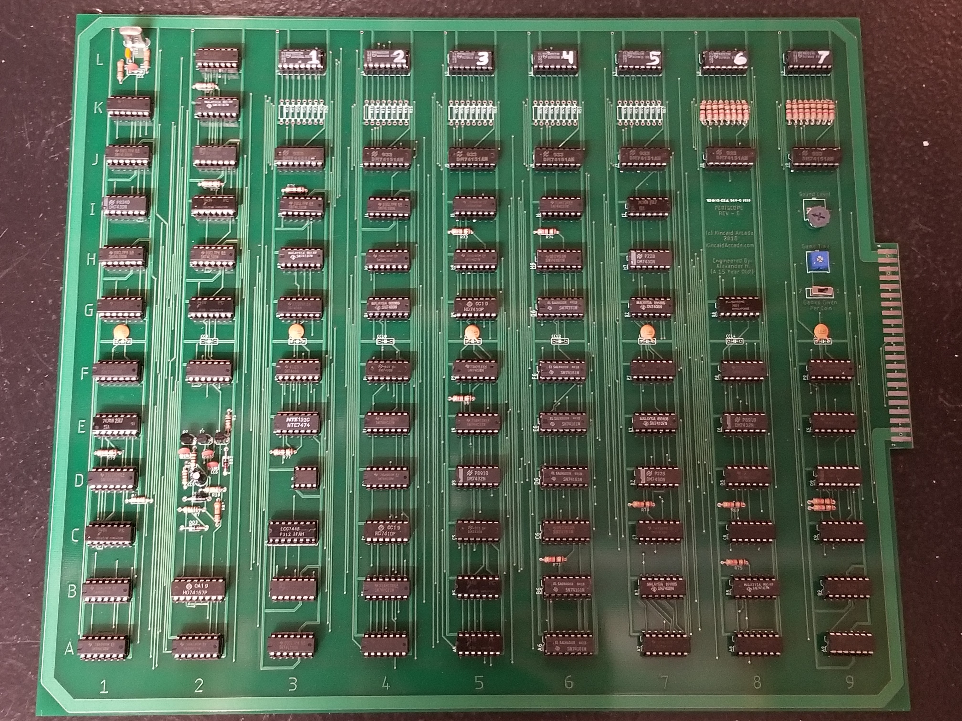
- Designing the REV-C Board:
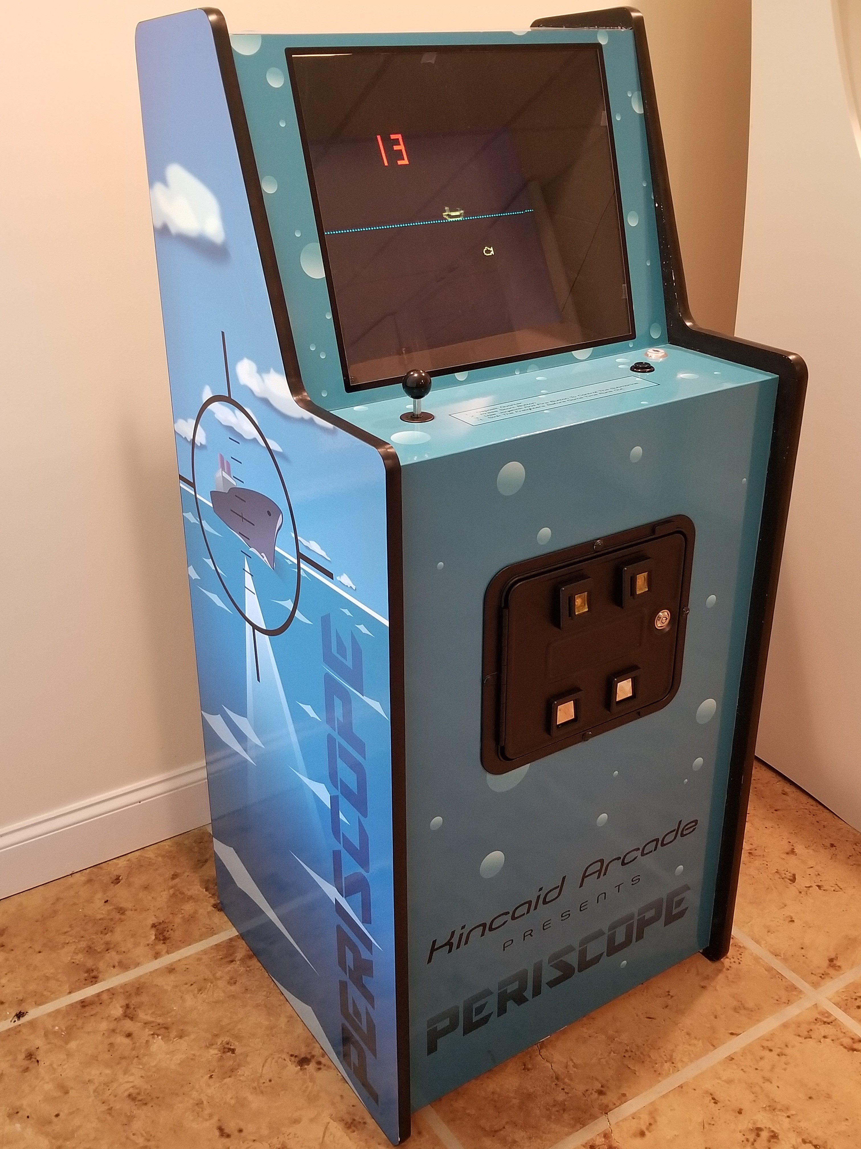
- Designing The Cabinet:
- Gameplay Videos:
- Reflection:
I have also included two schematics for your entertainment.
The REVISION-C has everything working, (minus the only PCB mod, a diode between COINNO on the edge connector and COINNO on the PCB.)
The PROTO-A schematic is where I threw most of my early ideas before I fully understood TTL. Almost nothing beyond the sync circuits actually works. It is still interesting from the perspective that it shows how much I have learned.
Here they are:
PERICOPE REV - C SCHEMATIC
PERISCOPE PROTO-A SCHEMATIC
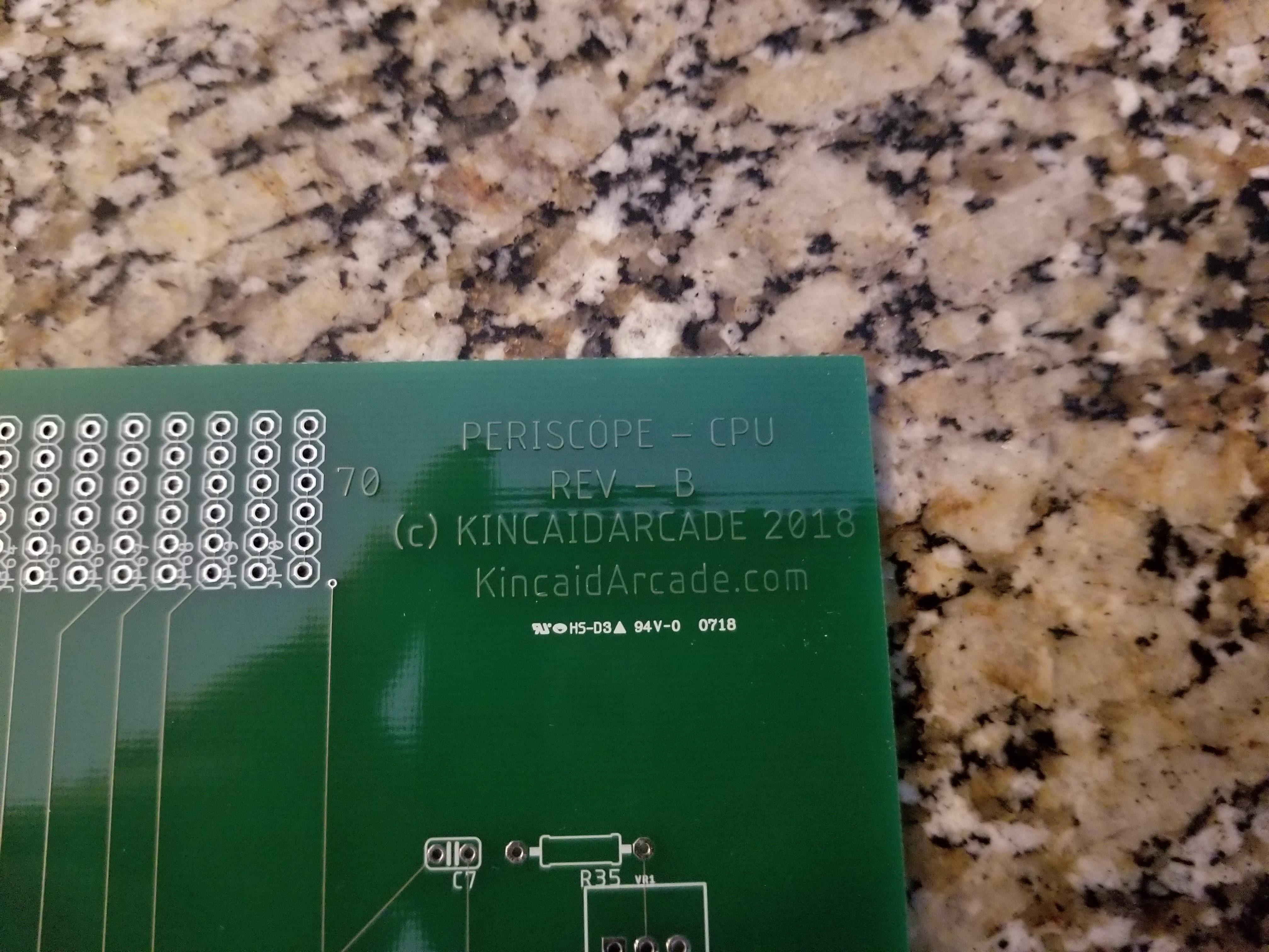
NOTE: REV-C chips and chip locations differ from all the other prototypes. The REV-C is used for most explanations because it is the most polished and simplified version of what is happening. (I reduced the chip count by about 70 when compared to the largest prototype. That's what happens when you use ALL the gates on a chip, instead of just one or two...)
If you are completely new to this, I suggest you read:
The Textbook Of Video Game Logic, Volume 1
And:
ATARI PONG E CIRCUIT ANALYSIS AND LAWN TENNIS
How I Came to Chose PERISCOPE as This Year's big School Project
Every year, my school has the Eden Exposition. It is like a science fair, but instead of forcing the students to do a bunch of STEM projects, the requirement is that each student spends 24 hours on a project using whatever gifts, talents, or abilities that God has given them. The school first explained why we have it when it started back in 2013 as such: "As Christians, we worship a creator God. Because we worship a God who creates, so we should also make (create) things." So the question, like usual, was: "What will my project be this year?"
In the years past, I did:
- 2013 - 2014 : An Autonomus Maze-Navigating Rover
- 2014 - 2015 : The Garden of Eden Pinball Machine
- 2015 - 2016 : An 8 x 8 x 8 RGB LED Cube
- 2016 - 2017 : An Electric Go-Kart
This year, we were actually planning on having me learn how to use a CNC machine, and using it to make a 7.5" gauge live-steam garden railroad locomotive. The more research we did, the more we realized that, although it would be doable if I did something super simple, ex. only 1 piston, it would be too expensive. With a little more than a month before the deadline for choosing a project, I suggested kinda sarcastically: Maybe I should do a TTL arcade game?
My parents actually liked the idea, and they said I could do that. "Wait, Really?"
"Yeah, sure!"
So my Eden project was chosen. (When I say Eden project, it is short for my Eden Exposition Project)
Well, almost. I still didn't know what game I was going to do.
Some time passed. About a month to the deadline for choosing a project. I was talking over my Eden project with my Dad, while riding in the car on the way to school.
He suggested: "You know? We've been planning to have a pinball build - off for awhile now, and we still haven't done anything about it. How about you have PERISCOPE be a TTL arcade game, and come up with another pinball theme?"
That was a great idea. I loved it. (Maybe my Dad only suggested that because he was scared that my theme might outdo his!)
Some Context Before Designing the PERISCOPE Logic Board:
With about 6 months before I had to show it off at the exposition, I had my work cut out for me. That was about how much time an engineer at Atari had, and I doubted that a 14-year-old would be able to do something that takes an engineer who went to college to do stuff like this less time to do it. Probably not. Better get started.
Fortunately, I had several advantages. I had a lot of expierience from when I unsuccessfully tried to clone PONG with 66 TTL ICs during the summer after I built the Garden of Eden pinball machine.
It worked, except for the fact that each player had 32 paddles. And that the clock signal would die whenever the ball hit a paddle. And that the paddles would stretch to the bottom of the screen. And that the score was being repeated everywhere. Although it had many issues, I still learned a lot.
My other advantage: The schematics of basically all the TTL games designed in the past. This would prove to be quite a valuable asset. I had basically no experience in TTL. This would give me a crash-course on it.
For all the hardcore history buffs among you, the practice at Atari for initiating new engineers was for a senior engineer to dump the schematics of a previous game into their lap. The newbie was expected to use them to give themselves a crash - course in how computer games were designed, using these schematics.
From my reading, the other suggestion I got was that you need to be familiar with your game to the point where you can play it in your head before you even start to program it.
Admittedly, when using TTL, it is easy to come up with a seemingly simple game idea, that is hard as rock to implement.
These were my technical ideas.
At the time, it should have occured to me that this sounds more like what a CPU game could do, not a discrete game.
Now, while writing this article, it occured to me that it could've been a game of Monaco GP or INDY 800-level difficulty. Although I knew basically nothing about doing this, I still shot for the moon. A little challenge is always good!
Time to start designing some circuits!
The Clock Circuit:
The clock circuit is located on REV-C and PROTO-A schematic page 1. This is the exact same circuit as in PONG.
When designing your circuits, the first thing you need is a clock circuit. It produces the clock signal, which is just a ~7 mhz signal. (It gets divided in 2 from the ~14 MHZ crystal.)
From this signal, nearly every other game signal will be generated. You cannot have a working game if your clock signal doesn't work.
The ~7 MHZ signal is determined by the resolution of your game. If you want a 455 X 262 pixel screen at 60 frames per second, ~7 MHZ works fine.
Do: 60*262*455, and you get 7,152,600. That is how we get ~7MHZ.
Horizontal Sync Generator:
The Horizontal Sync Generator is located on REV-C and PROTO-A schematic page 1. This is the exact same circuit as in PONG.
Next, you need to take your clock signal, and run it through a series of counters and flip-flops (J1, J2, and K2) to count out the horizontal pixels.
The width of each frame is dictated by the NAND gate at I1. Add 256H + 128H + 64H + 4H + 2H, and you get 454.
This dictates when the signal HRESET (Horizontal Reset) happens. Horizontal Reset just means the beam of the CRT shifts down a line, and starts drawing out the next 455 pixels.
We get 455 from 454, because it takes the time of 1 pixel from the previous 454 happening for HRESET to trigger, hence the game screen is 455 pixels wide.
Vertical Sync Generator:
The Vertical Sync Generator is on REV-C and PROTO-A schematic page 2. This is the exact same circuit as in PONG.
The main output from the Horizontal Sync Generator is HRESET and /HRESET. (The / indicates it is the inverted version of the signal.)
We use HRESET because it happens only when a horizontal line has finished drawing, indicating that it is starting the next vertical line.
This is fed into a chain of counters and flip flops (H1, H2, H3), to count out the vertical lines.
The game's vertical resolution is 262 lines. We get that by adding them together at NAND gate G2. (256V + 4V + 1V = 261)
This dictates the signal VRESET and /VRESET, the outputs of I2. We get 262 from 261 because it takes 1 vertical line of time for the VRESET signal to happen. (And the /VRESET signal to do the opposite.)
When VRESET happens, it signals to the monitor to start at the top again. It also signifies a complete game frame.
Generation of Blanking Signals:
The circuits responsible for generating the blanking signals are located on REV-C and PROTO-A schematic page 3. This is the exact same circuit as in PONG.
A blanking signal is a signal that dictates what part of the frame is reserved for sync signals. They are typically located just barely offscreeen.
Because the BLANKING signals are located just offscreen, they are perfect if you need to check if a game object hits a side of the screen. (1/4/2022 Using blanking signals for object collisions is less than ideal. If you do, make sure to gate the objects out of blanking so they don't get read by the monitor as the sync signal.)
Because I was still learning how TTL worked in this stage of the project, I was just copying circuits from PONG. (Sync stuff - why reinvent the wheel?)
I still don't fully understand what is going on that creates the VSYNC and HSYNC pulses, or how this method was chosen, but I do understand:
The gates at F1 (B and C) form a reset - set flip - flop.
The gates at G1 (A and B) also form a reset - set flip flop. VRESET sets VBLANK high, and after 16 vertical lines, 16V goes high, and it resets it back to 0. This creates your Vertical Blank signal. If you wanted to use /VRESET and /16V then switch the NOR gates to NAND gates. (Functionally the same thing.)
G4A and G3C create an XNOR (Exclusive NOR) gate, which keeps the /VSYNC and /HSYNC pulses separate, which is what the monitor needs. If you used VSYNC and HSYNC, you could eliminate G3C, but that would use more gates in the end.
Sync Signal Inversion:
The Sync Signal Inversion circuits (just inverters) are located on REV-C schematic page 4.
I designed this, and I basically just used this page to consolidate all of the signals I have inverted onto a page so I don't accidentaly use extra inverters when I already have the inverted signal.
On the prototype CPU board, I had many more inverted signals, but most of them weren't used in the final product so I just removed them and kept what I needed.
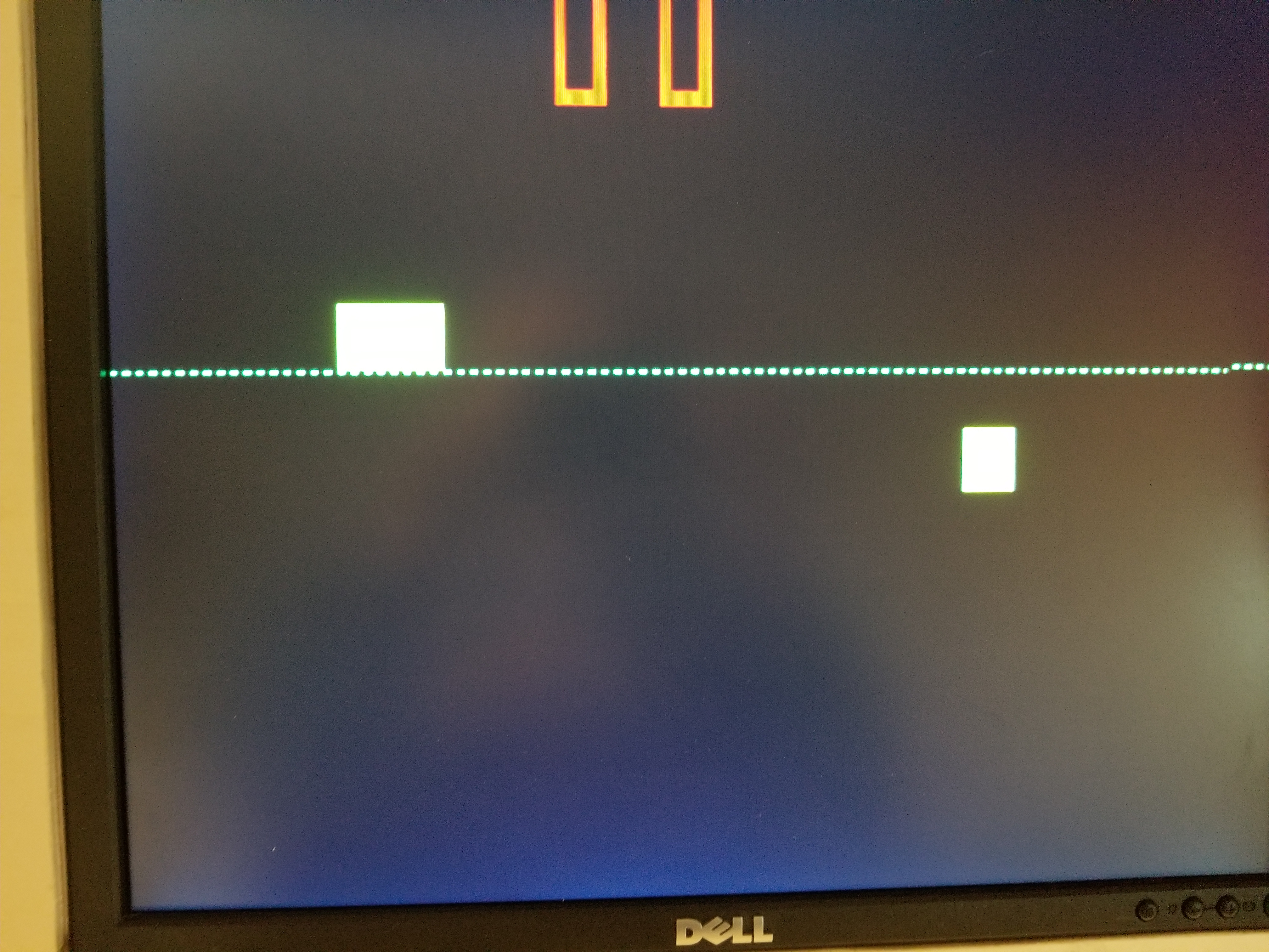
Ocean Generation:
The Ocean circuit is the very first TTL circuit I ever designed myself. It is located on REV - C schematic page 5, and PROTO-A schematic page 4.
I originally tried using the net circuit in Pong, and just changing the H and the V signals. It looked like this:
Not quite what I needed.
So, I drew out the signals for 1H, 2H, 4H, etc. as well as the V signals on graph paper. I had an idea: Define the vertical position with a NAND Gate (F4) and an Inverter (G4), then AND it (F5) with 2H, and then I would have my ocean!
It worked, first try!
Here is the current prototype of the time:
If you look closely at the board, you can see that I had unsucessfully tried to do VGA. It proabably would've worked if I changed the SYNC generators to do 800 X 600. I think I would need extra flip-flops, a 57.6 MHZ crystal and another 7430 to do it.
To do it well, I probably would need to change the asynchronous 7493s to synchronous 74161s. That would reduce positional error for game objects, because it would eliminate the 7493's propagation delays.
1/4/2022: I've actually done more research on this because it was relevant to a candidate for a project that I was thinking of doing over the 2021 Christmas break, and I have determined that a 640 x 480 at 60 fps display with TTL is possible at an 18,432,000 Hz clock. However, that is literally the upper speed limit of common TTL chips.
RGB OUT:
This was one of the circuits I designed next. It is located on REV-C schematic page 5, and PROTO-A schematic page 13.
I was going to use a video converter because finding a composite monitor is just too hard these days. If the RGB output worked with Color Gotcha, then it would certainly work with PERISCOPE!
The circuit really just consists of a bunch of OR gates. I OR together game object signals into R, G, and B, and send it to the video converter.
It didn't work at the time because I left many inputs floating. I fixed that on the next prototype by adding pulldown resistors on the unconnected inputs. (The inputs for game objects I hadn't made yet.)
Freighter Motion: (Attempt 1)
This circuit is located on PROTO-A schematic page 5.
This circuit never worked. Why? I *think* it was because I used pulldown resistors to ground. (I learned the hard way: NEVER DO THAT!) If I hadn't used them, then maybe it would've worked.
There were probably other errors I could've come back later and fixed, but I decided that starting from scratch would be better.
Here is what it looked like:
The Coin/Start/Game Circuit: (Revision 1)
The original Coin/Start/Game Circuit can be seen on page 9 of the PROTO - A schematic.
The revised and fully working Coin/Start/Game Circuit can be seen on pages 6 and 7 of the REV - C schematic.
It was copied from Anti-Aircraft II, because I still didn't understand too much about how TTL works. I do, now.
If I had to design another game, (and I really am considering it...) I would design it from scratch, and do the antenna circuit using all TTL.
(On the REVISION - C schematic,) D1A & B function as a debounce for the leaf switch in the coin mechs.
C1A & B function as a toggle that only toggles its outputs when the switch has been pressed. 128V is used to further debounce the switch.
The flip flops at E1 are responsible for keeping track of whether or not the game's credit light should be lit.
Looking at page 6 alone would have this circuit not make sense, however, when looking at F5C on page 7, the circuit makes sense because the GAME signal toggles once every coin drop.
F5 and E3B on REV-C schematic page 7 handle the start button. E3B only toggles if the start button has been pressed AND there is not a game in progress.
(I messed up the naming of the GAME signal, GAME is actually when ATTRACT mode is on and /GAME is if a Game is in progress...)
When START and /START trigger, E3A resets to having a game in progress. It also resets D3, the only 555 timer in the game. The 1 Mega Ohm potentiometor determines how long it waits before the output goes low, which is then inverted by D1E, which clocks a "1" into E3A, which ends the game.
The circuit looked like this:
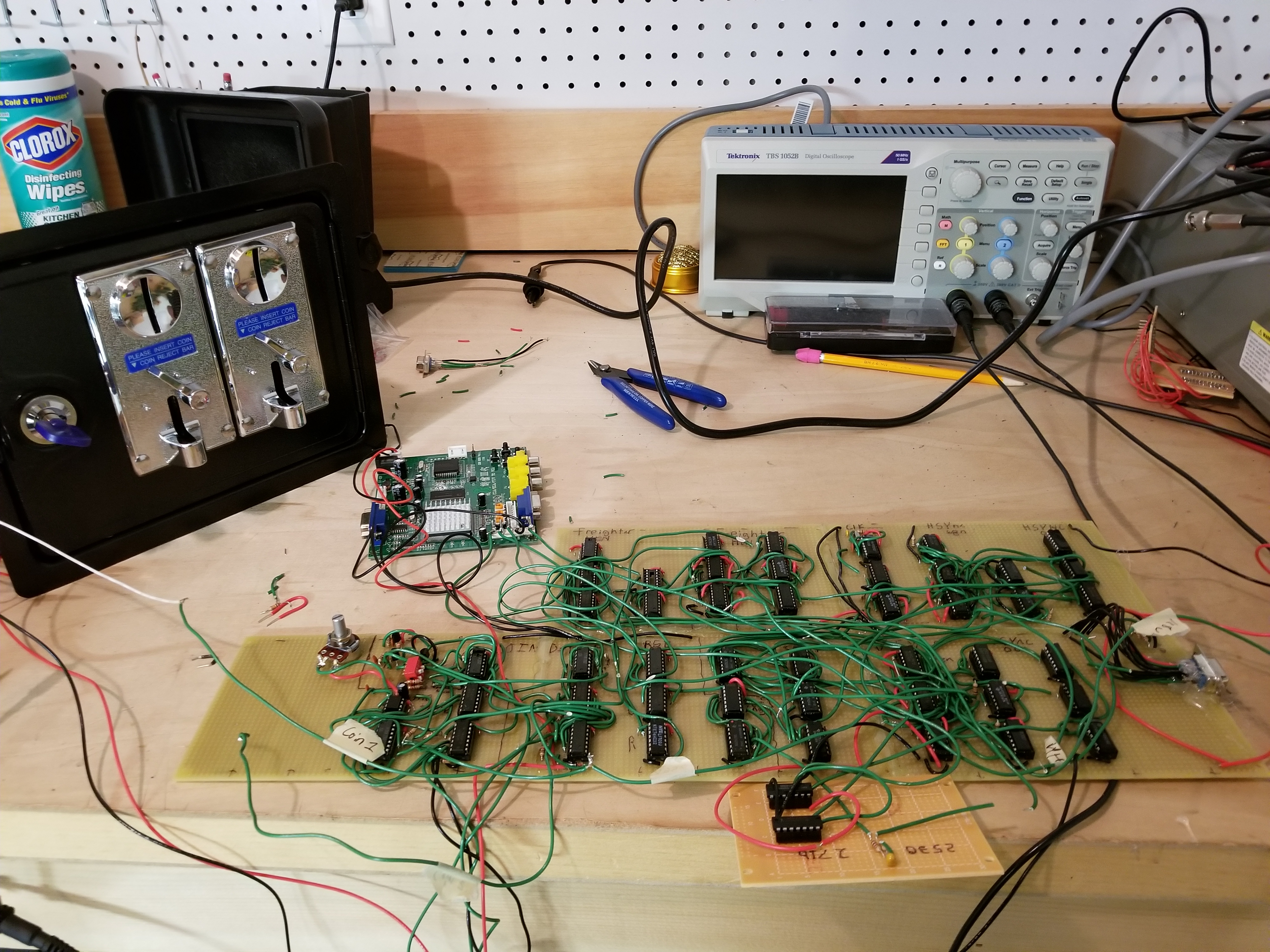
Pro Tip: Avoid those cheap Chinese coin doors & coin mechs like the plague! Both coin mechs arrived defective. Both would not output ANY signal when a coin pased through, and one would not even trigger the lockout coil when a good coin went through. One would not trigger a coin counter, either.
Buy a reproduction Wells-Gardener or one of these instead.
Score Counting and Score Segments:
The Score Counting and Score Segment circuits are located on pages 8 and 9 of the REV-C schematic, and page 11 of the PROTO-A schematic.
This was the last circuit I put on the PROTO-A board before designing a PCB so I could ditch the prototype. (It was very finicky...)
I designed the Score Counting circuit myself. (It is rather innefficent... but I am proud of it, none the less.)
The Score Segment circuit was taken from PONG, because I didn't understand what it did at the time. I understand it now.
In the score counting circuits, A1C & D and A2 make up two 5-input AND gates. They determine horizontal windows (synonyms: Enable, Position, etc.) of the TENS and the ONES digits.
The 4-input AND at B1B determines the vertical score position. A1A & B AND the TENS and SCOREVEN and the ONES and SCOREVEN signals together, making the ENTENS and ENONES enable windows.
E5B then ORs these signals together to make the SCOREEN (pronounced "SCORE EN") signal, which enables the 7448.
B3 and A3 count the score tens and ones places. The Start signal clears both counters at the start of every game, and B4D ORs the START and ADDTENS signals, also allowing the ones place to be cleared when tens are added.
The 4-input AND at B1A determines when it is time to add one to the tens place, and when to reset the ones place.
The 74157 at B2 takes the BCD outputs of B3 and A3 and selects between them using the ENONES signal. It then outputs the BCD of the counter it has chosen, (tens or ones) which is then sent over to the 7448 at C3, which converts the BCD to 7-segment display signals.
The Score Segment circuit just puts a 7-segment display on the screen.
C4, C5 and A5A all act as enables for each segment of the 7-segment display, by using the SCOREA through SCOREG signals.
A5B and D1 make up a circuit which creates a bar 16H wide and 4V tall, that takes up an 8V area. This is used in segments G and D.
B5C and A5A (G and D segment mixing, respectively,) use the 16V and /16V signals to keep their segments from showing up in each other's space.
K1B and G1C creates a vertical window that occupies 4 horizontal pixels in an area that is 32 pixels wide. (one cycle of 16H is 32 pixels wide. Off for 16 horizontal pixels, on for 16 horizontal pixels.)
Like the circuitry for segments D and G, the B and C segment data mixers use 16V and /16V to keep their segments from being repeated / showing up elswhere.
The circuits that produce the F and E segments are similar to the B and C segment circuit, but it uses the 3-input NOR at A4A to create a vertical window that occupies the first 4 pixels in a 32 pixel period.
B5B is responsible for mixing and enabling signals to create the A segment. It uses the 3-input NOR gate at A4B to create a window that is 16H pixels wide, that occupies the first half of a 32-pixel area, that is 4V pixels tall, that occupies the top half of an 8 vertical pixel area.
The 8-input NAND at C5 coupled with the inverted outputs of all the segment data mixers acts as NOR gate, even though it is a NAND gate.
That outputs the SCORE signal, which gets mixed into the RED output, which is then displayed as red on the monitor.
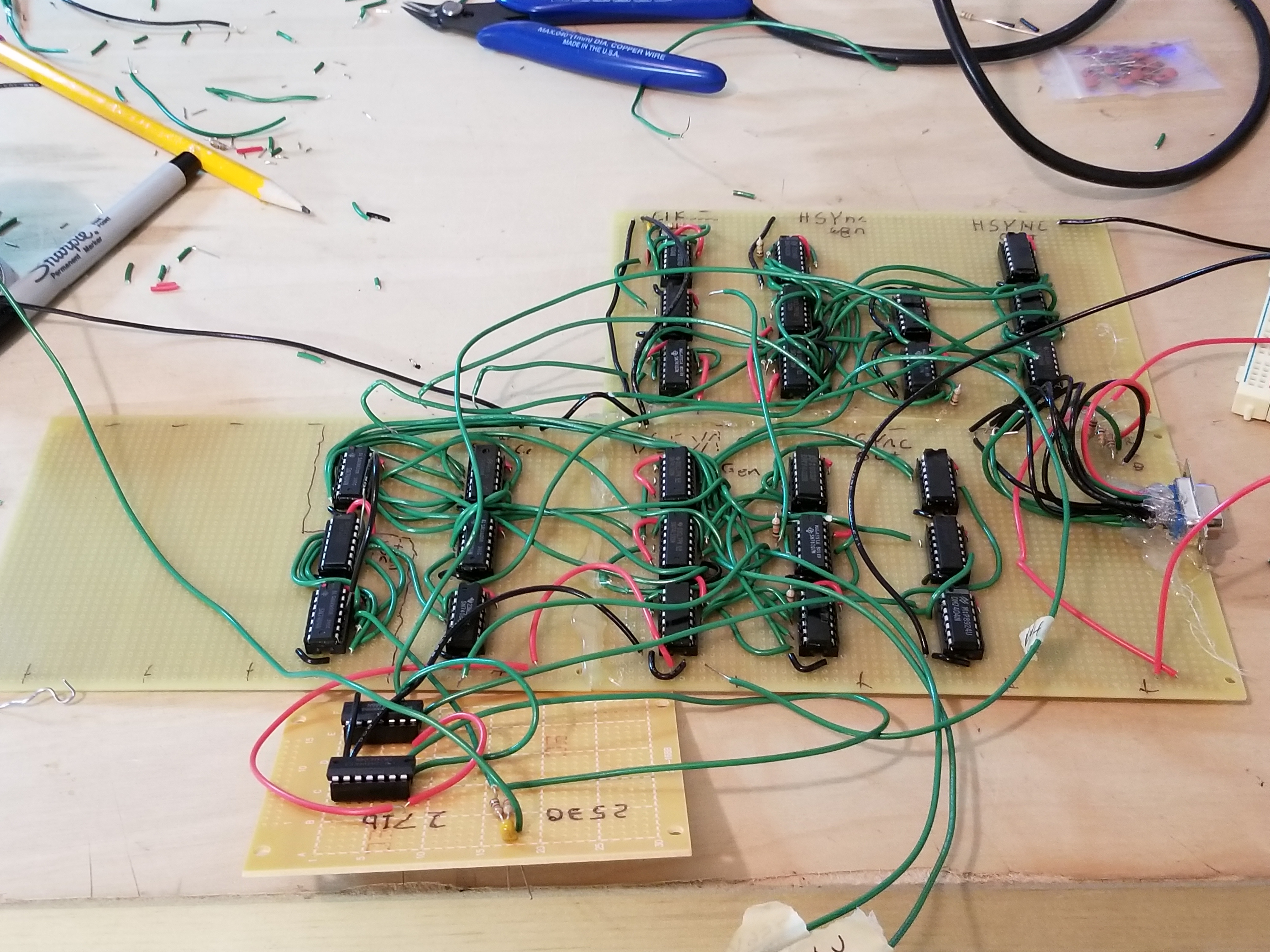
After soldering all that up, the circuit board looked like this:
(All the SCORE circuitry is on the small daughter-card on the left.)
When testing it the first time, it was apparent I switched the enable wires for the G and B segments by accident.
I also had to redo the ADDTENS trigger because it was triggering on the "9" and not when there was a "10" in the ones digit.
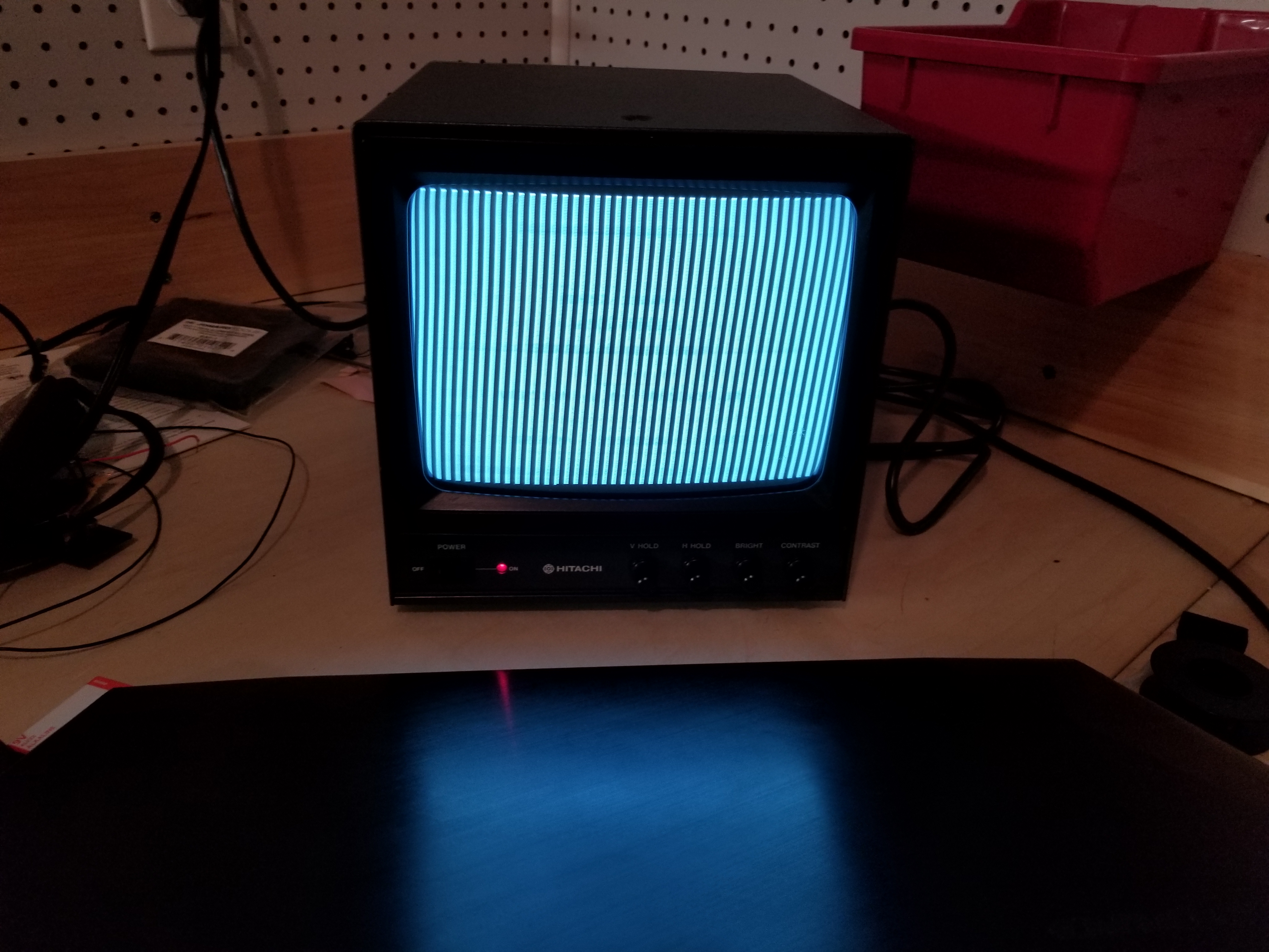
(Every time you see the video output on the CRT, It means I bypassed the video converter and soldered up a sync summing resistor network to make it suitable for the monitor.)
Here it is after I fixed all that:
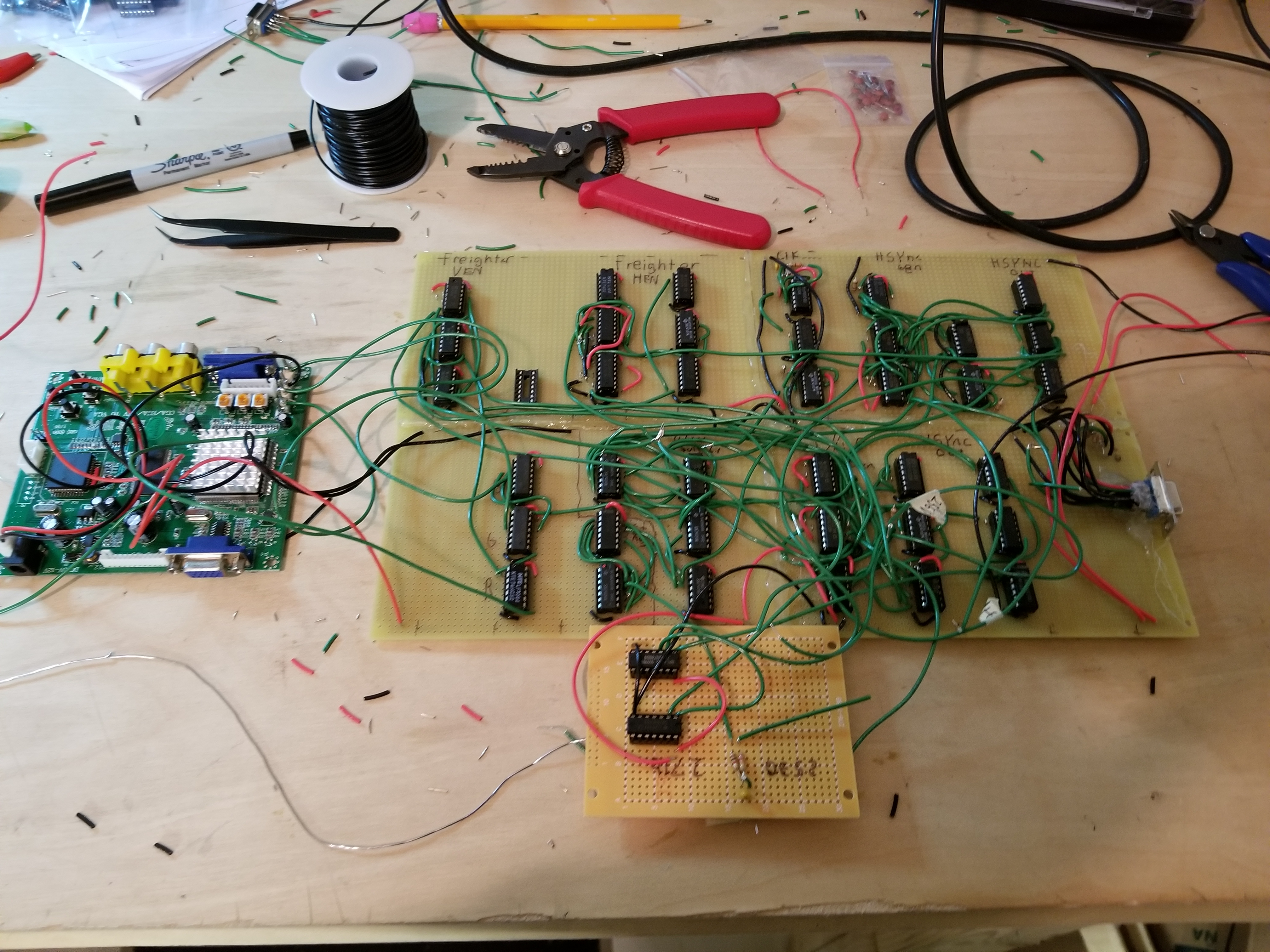
Designing The First Prototype PCB:
Designing a board and ditching my prototype was a suggestion from my Dad.
My prototype was getting very large, and circuits were just shutting down from the sheer amount of wires causing intereference with each other.
With a next revison PCB as a goal, I designed one last circuit: the SCORE circuit. (The two circuits we just went over.)
Using Eagle, I copied, pasted, and renamed the schematic to become the schematic for the CPU board.
(The game does not use a CPU, I erroneously refered to it as the CPU board because I misunderstood that for a TTL game it is NOT called the CPU board since the games don't have a CPU. I thought that people still referred to them as CPU boards anyway; although any who did were wrong. I can't really correct this since it's already been silkscreened onto the boards.)
I deleted all the schematic pages with circuits I was ditching. I clicked the "create board from schematic" button in Eagle.
From there, I spent several days figuring out the locations of the chips, how to make large power and ground traces, where a 22-pin card edge connector part was located, how to use the autorouter, etc. (I didn't optimize the board so that all the gates in all the chips were used. I didn't know how to move gates between schematic pages. Now I do.)
Then I had to figure out how to make gerber files. That was... fun.
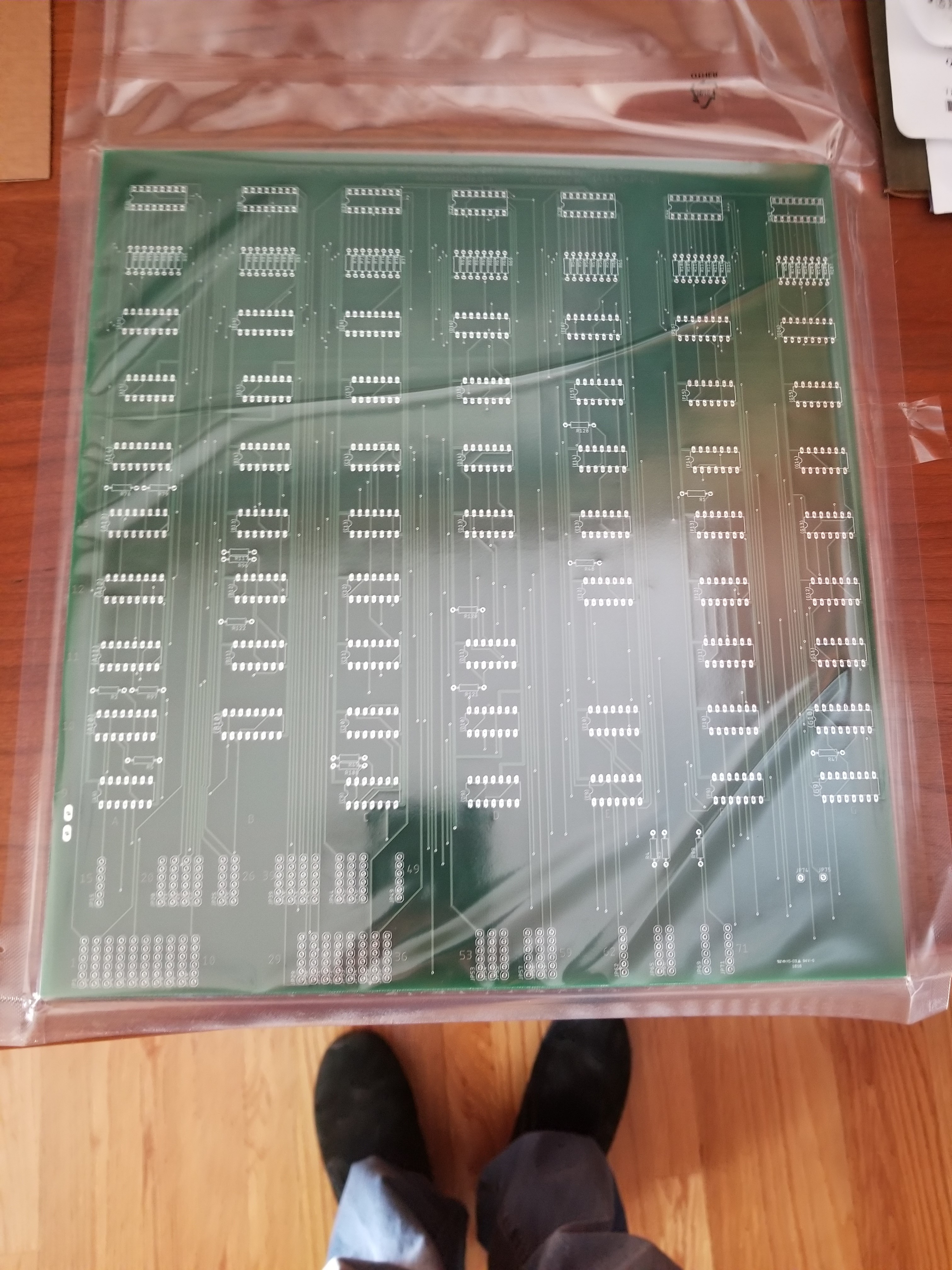
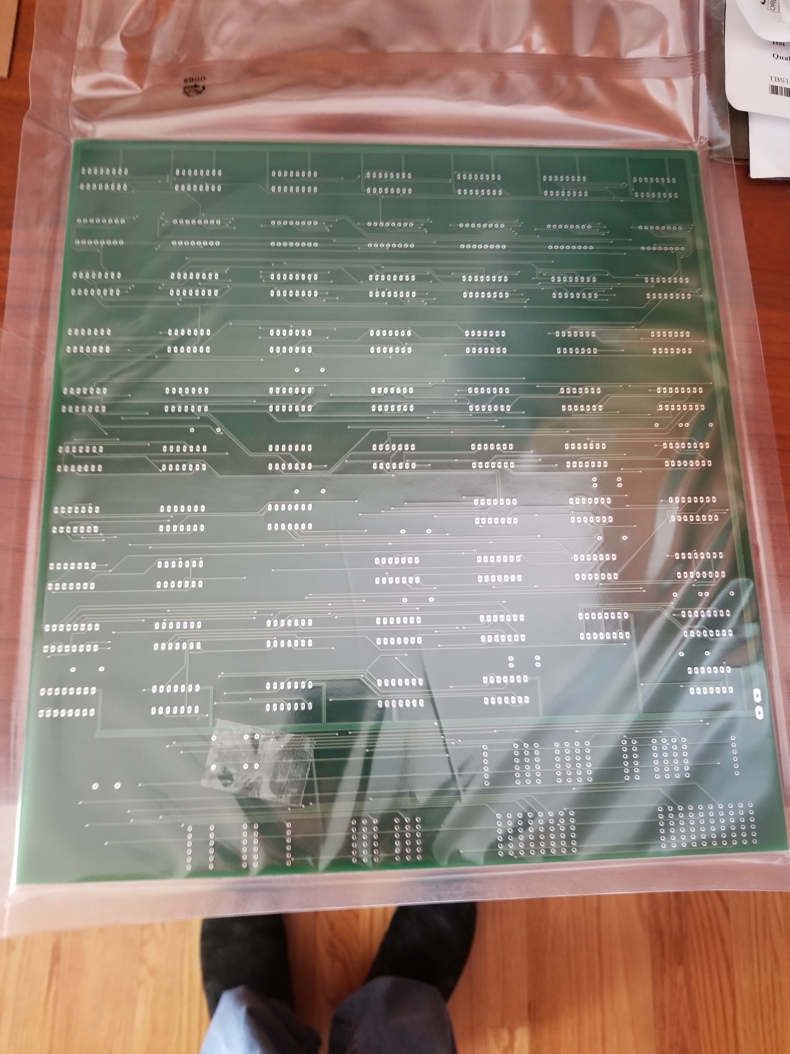
Next, like everyone, I looked for a cheap and high-quality prototype and production pcb manufacturer. I found Quick Turn PCB. ABSOLUTEY LOVE THEIR SERVICE!
They are based in Bucheon, South Korea. Their prices are the cheapest out there. (Except for 2 Chinese places... But I think we can all pay a couple extra dollars on our whole order to have the guarentee that the Chinese aren't going to clone it and sell it for less...)
One of the things that surprised me, was that they manufacture one extra board on the total number of the order, in case one of the boards tests bad. That way, they don't have to delay to fabricate a new board. In the case that they all test good, they send you the extra board anyway!
This is all from personal expierience, I am not being paid to advertise for them. I have done more than 4 orders with them, from greater than 12" x 12" to under 2" by 2" boards. No complaints.
Anyway, after filling out the stuff on their online quote form, selecting a price, ordering, PayPal-ing Geum Han (or is it Han Geum?) the money for the order, he sends me an e-mail that I didn't include drill files. So, after making them and sending them to him, he sends me an e-mail about an hour later telling me that the boards are being fabricated! That was fast! They have always finished producing them 3-4 days faster than the timetable I selected...
Absolutely amazed with the boards when they arrived:
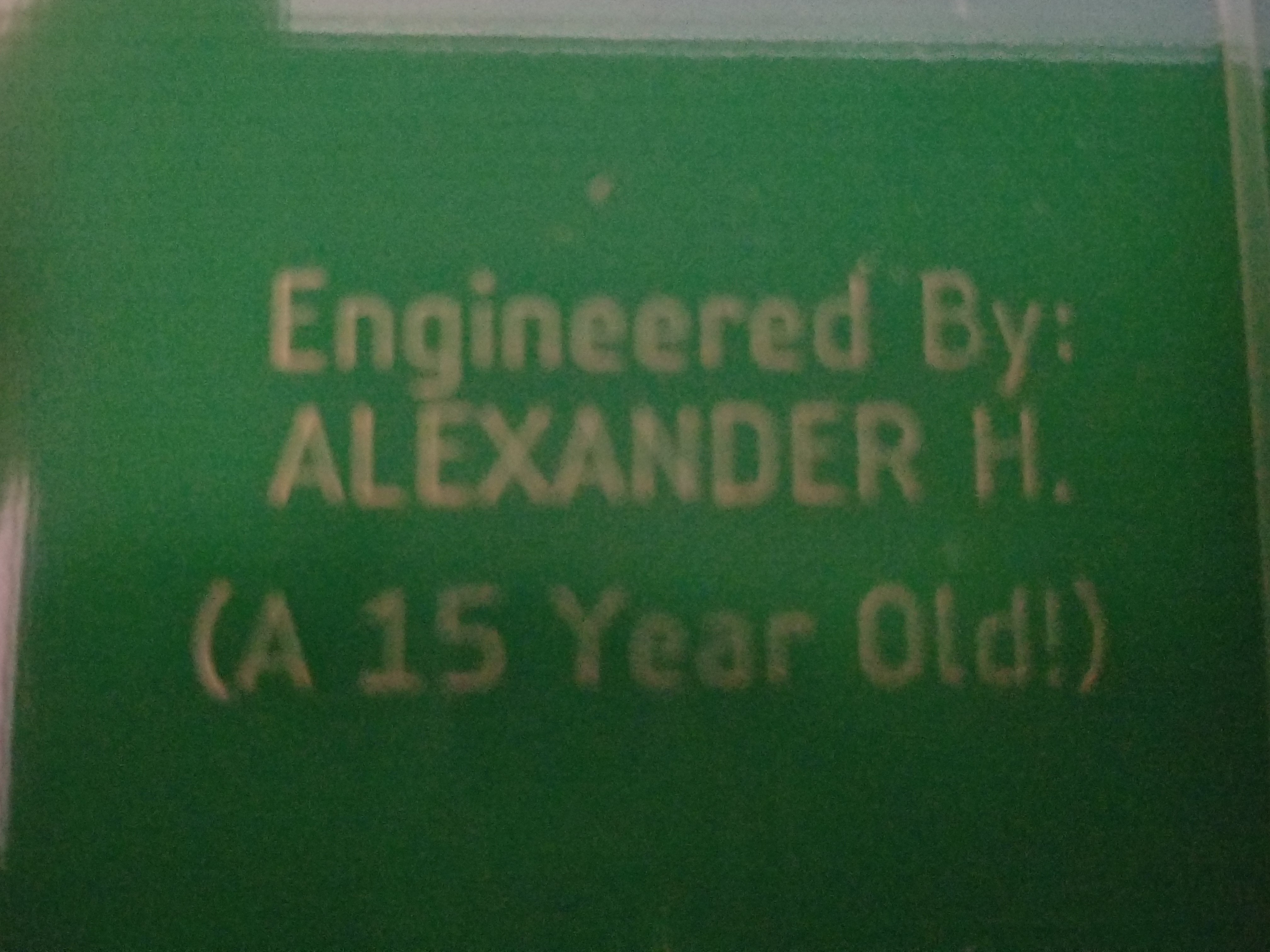
(I am embarrased to say I got my own age wrong... I was 14... this is why you check your work...)
Pro tip: Socket all your chips across all prototypes. Then you can swap the chips over. It saves you money, especially considering a socket is $0.14 and the average chip is more than $2.00. Also: Why buy sockets in small quantities? I have used over 600 sockets in the course of this project.
After I soldered it up:
Jameco Electronics has become my one-stop-shop in the duration of this project and future projects.
Because I designed this board with the intention of using it in another prototype, I added lots of holes for major (and some minor) signals. They can be seen at the top of the board in both pictures.
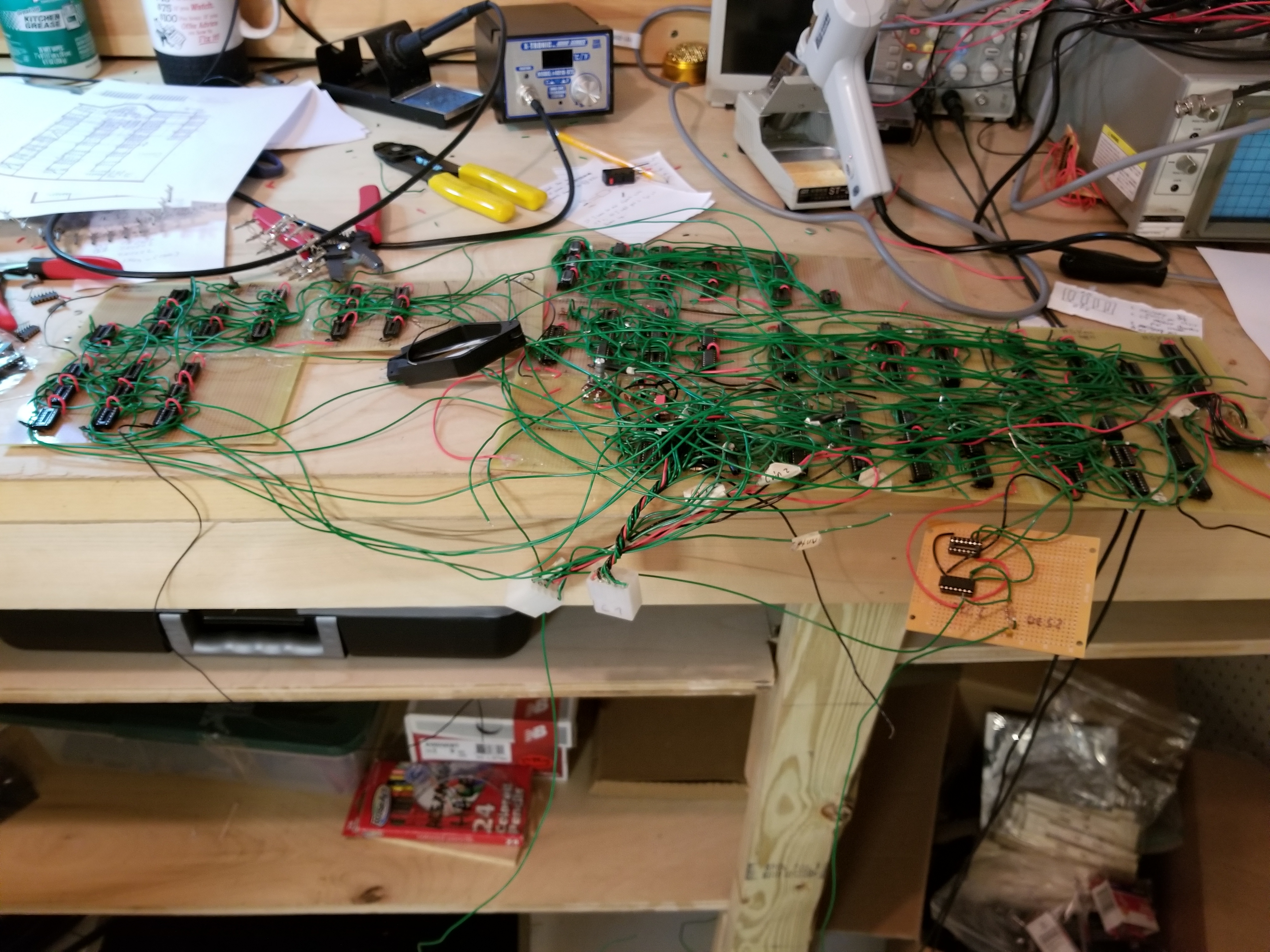
Time For Some Motion Circuits! (The Submarine)
The motion circuit for the Submarine is located on page 14 of the REV-C schematic. I designed something that didn't work on page 6 of the PROTO-A schematic.
For the record: I'm not sure what I dislike more. Motion circuits, or ROM / PROM reading circuits. Either way, I still consider both of them the bane of my TTL existance. Why, you may ask? I will grant you that the motion circuit can be quite simple -- just requiring three chips -- but don't let that fool you. There are so many possibilities for error with these circuits.
One time, I couldn't figure out why the motion circuit I took from Space Race wasn't working. I soldered it up elsewhere on the board, and it worked the first time. Apparently the lack of filter capacitors on the board was allowing all the wires to create noise on the voltage line, messing up the timers. This is why you need your .1uf filter capacitors.
On the other hand, ROM / PROM reading circuits get very repetitive. (Although, I could've saved myself the hassle if I used a 2 kilobyte PROM instead of x7 256-bit PROMs) Don't get me wrong, I love that when they fail, they are easy to troubleshoot because they fail in a very visual way. If I miss a wire, a row of pixels will be missing, etc. They are the bane of my TTL existance because of the sheer amount of wires that need to be soldered. I routinely forget to solder wires I put in... and there are a LOT of wires in these circuits...
Anyway, bias for motion circuits aside, they are quite necessary for a TTL game. I don't think there is a TTL arcade game out there without a moving object.
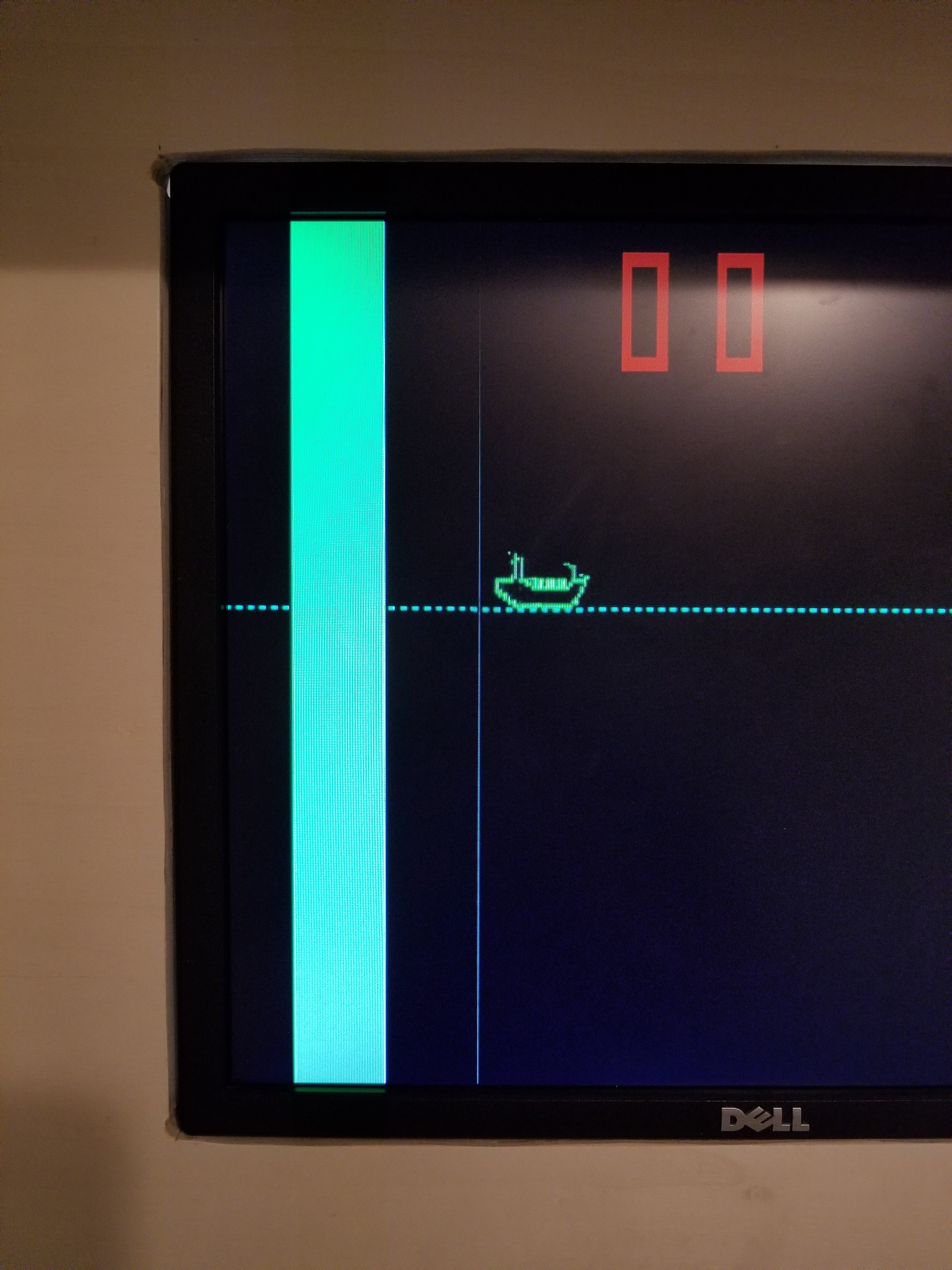
The motion circuit for the Submarine is the exact same as in Space Race. (With some slight changes.) I designed the control circuit myself. The circuit is comprised of counters C6 and D6 (74161s), and the NAND gate at C8D. Counters C6 and D6 count out the pixels for the screen. When it reaches 16 pixels before the end of the count, the RCO of D6 goes high for 16 pixels. The illusion of motion is produced by presetting these counters to skip a count or count extra. Skipping a count makes it look like it is moving upward, counting extra makes it look like it is moving downward. When the Sub is not moving, the control circuits keep the presets set to the number of pixels on the screen.
Aside from the control circuit, there are several other mini circuits that help generate the submarine.
D7 and D8F take signals from the Horizontal Sync Generator and produce a vertical window 16 pixels wide. (A vertical window stretches to the top and bottom of the screen.)
C7C & D take the Submarine H (the vertical window), V position, the graphics, and combine them to create the Submarine.
I soldered up the motion circuit correctly. (Except for one wire.) This showed up:
When I first saw that, I screamed and shouted for joy! I was so excited! Even though that technically wasn't what I was expecting, I just proved I could do a motion circuit! After fixing the wire I got out of place, (I accidentally connected SUBVEN to pin 15, C6,) this appeared:
Pro tip: solder up switches to all the presets before designing a control circuit. Try each combination, and make note of the direction and speed. It will help.
Now, I need to actually be able to control that without flipping switches.
The next step: the control circuit.
The Submarine Control Circuit:
The Submarine Control Circuit is located on page 15 of the REV-C schematic. I designed something that didn't work on page 6 of the PROTO-A schematic.
For my sake, let's pretend everything was just dandy and I got it the first time. (And that it didn't give me problems for several weeks.)
I had many funny problems along the way, such as:
- Submarine moves up when the joystick is pressed down.
(And it's not as simple as switching the wires on the joystick, then other problems arise.) - Submarine does not start below the water.
- Submarine does not collide properly with the ocean surface.
- Submarine does not collide properly with the ocean floor.
- Submarine doesn't move at all.
- Submarine can be moved in attract mode but not during the game.
The part of the control circuit that handles the joystick input is relatively simple, using just 7 gates. The gates C9A & B, D9A & B, L2D, F3F, and C8A take the joystick input, and convert it into the A and B inputs for presetting the motion circuit.
E9A and E9B take V signals from the Vertical Sync Generator and use them to create the vertical positions of the Ocean Floor and the Ocean Surface collisions.
C9C & C9D OR the collision signals and the attract signal (GAME) to create the conditions for when the SUB should not move.
C7A & B, as well as H3B make up the circuit that keeps track of the REPOSSUB signal. If the sub is not under water, REPOSSUB is a 1, until the sub is moved under the water. This circuit is only ever used on powerup. I designed it because the motion circuits always start drawing the position of the Submarine at 0, which is at the very top of the screen, and above the water. A flying submarine sounds like something Adam Young would sing about.
It moves the submarine upward until it hits the ocean collision. (Under the water)
When I finished soldering all the submarine stuff up, it looked like this:

The (Working) Freighter Motion Circuit:
The (Working) Freighter Motion Circuit is located on page 10 of the REV-C schematic.
I was not sure how to do the Freighter Motion Circuit. I had never done a 32-pixel horizontal motion circuit before. I've really only ever seen motion circuits produce a window of 16 or less pixels.
I figured that Atari probably already figured it out, and I'd just have to find it. So I thought to myself: what game might have had a 32-pixel motion circuit? The only answer I could think of was Shark JAWS. Unfortunately, the schematic on the internet had one faded page, which just so happened to contain the motion circuits. On the bright side, that forced me to design my own solution. I am quite pleased with what I came up with.
I started by copying the motion circuit from Anti-Aircraft and soldering it up. It worked, but it only produced a 16-pixel wide window, so I still had to figure out how to double it. I figured I'd just throw a flip-flop on the HEN (Horizontal ENable) and turn 16 into 32.
It didn't actually work. Since the HEN signal only happened once a frame, doubling it meant it would stretch off the screen and into the next frame.
The window the motion circuit created was just over half the width of the screen. (256 of 455)
Wanting to cop-out, I asked myself if I wanted to change the freighter to an aircraft carrier. I decided against it, because I would need to use x32 82S23s to store the graphics for it. (If I did 32 by 256). I figured it would be simpler to just figure out how to make a 32-pixel motion circuit.
I'm glad I stuck with the freighter -- I would've needed a ROM board otherwise. Needing x32 82S23s and x32 74151s, as well as AND gates and OR gates to mix and select which PROM, AND space to put 8 pull-up resistors for each PROM would've led to an expensive circuit board.
That would be more than 64 chips, and an extra 32 locations for the resistors. (After quickly designing it in my head,) I guessed it would probably be closer to 90 chips. Then I realized that I still needed an explosion graphic, so make that 180. Then I would need 64 banks of eight resistors for the PROMS. Obviously, there's got to be a simpler way to do it. The REV-C board only used 80 chips.
I had no idea how to use TTL to turn a 16-pixel motion circuit into a 32-pixel motion circuit. So, I tried an unconventional idea I had awhile back: rather than input the CLK signal, input 1H instead, and remove a flip-flop that Atari used to increase it to a horizontal resolution of up to 512 pixels / positions. I could do all that because 1H takes twice as long as the CLK signal to cycle once, so therefore the length of the freighter should be doubled, as well as the length of the motion circuit. (A 256 pixel / positon resolution with the CLK signal vs. one of 512 with the 1H signal.) The only drawback is that it will count by two pixels. It isn't noticeable, and is a good speed.
Sure enough, it worked:
In order for this to show up, I had to solder up a few extra circuits.
The 4-input AND at A7A is used to determine the vertical position of the Freighter, to be set on the top of the water.
B7A (AND) is used to combine the H and V position of the Freighter to make the enable window as seen in the picture above.
B7D (AND) combines the window (FREIGHTEREN) with the PROM data, to create the freighter image. (DFREIGHTER, Data FREIGHTER.)
A8A (AND) combines the Freighter's data with the VISIBLE signal, which determines whether or not the Freighter is shown on the screen. (It wouldn't be shown if it had just been blown up and was moving back to the start position.)
The inverter at G3E inverts the signal for the Freighter's horiziontal position. This outputs /FREIGHTERHEN, which is used to inhibit the Freighter Graphic Pixel Counter.
The Freighter Control Circuit:
The Freighter Control Circuit is located on page 11 of the REV-C schematic. I never got far enough to design this on the PROTO-A schematic.
The beast of a circuit that kinda looks like a cross-section of a Valor-Class cruiser is responsible for controlling Freighter explosions.
A7B is an AND gate, and it checks if:
- The Freighter is invisible, AND
- If the Torpedo collided with the Ocean, AND
- If the Torpedo collided with the Freighter's horizontal position when it hit the Ocean
If all those conditions are met, a signal is sent to B7B, which checks if the Freighter has been hit AND if the freighter is already not blowing up. I added this because a good player could keep hitting the freighter with the torpedo and keep resetting the explosion counter and racking up a huge score.
The output here is then inverted by G3F, (creating the ADDPOINT signal) to satisfy the falling-edge triggered score counters.
Anyway, the output of B7B is sent to B4A which ORs it with the ENDEXPLOSION signal, which allows either case to toggle the flip-flop at B8B, which keeps track of whether or not an explosion is active.
B7C is an AND gate which checks if an explosion is in progress, AND if a frame has happened.
B9 and A9 are counters that are used to count frames. (Using VRESET) Because VRESET happens ~60 times a second, I have the counters count it out 64 times, creating an explosion length of just over a second. When it reaches the 64th count, it activates the ENDEXPLOSION signal, which resets the counters and flips B8B back to no explosion.
A8C & D are set up as a 3-input AND gate, which checks if the Freighter has hit the STARTLINE while invisible.
The STARTLINE is defined in page 19, at the top left.
The 4-input AND at H4A takes signals from the Horizontal Sync Generator to create a fixed position on the screen known as the STARTLINE. (The STARTLINE is an area at the left of the screen that is used in determining if the Torpedo needs to reset to the Submarine and if the Freighter needs to become visible.)
I did some jumpering and modifying to show the STARTLINE area:
(The little spike to the right is part of the STARTLINE and is caused by the propagation delays of the 7493s in the Horizontal Sync Generator.)
A8B checks if an explosion has ended while the Freighter was visible. (For the sake of my game's circuitry, I count the freighter as visible when it is blowing up.)
B4B is an OR gate that allows the flip-flop at B8A to toggle if the Freighter needs to be made invisible, or if the freighter needs to be made visible.
B4C and K1D form a little circuit that controls one of the Presets in the freighter motion circuit.
Because the Freighter Motion Circuit uses CLOCK and not VSYNC for counting pixels, the Freighter moves at lightspeed.
The result of these two gates is the freighter not moving except for the short duration of the VRESET signal.
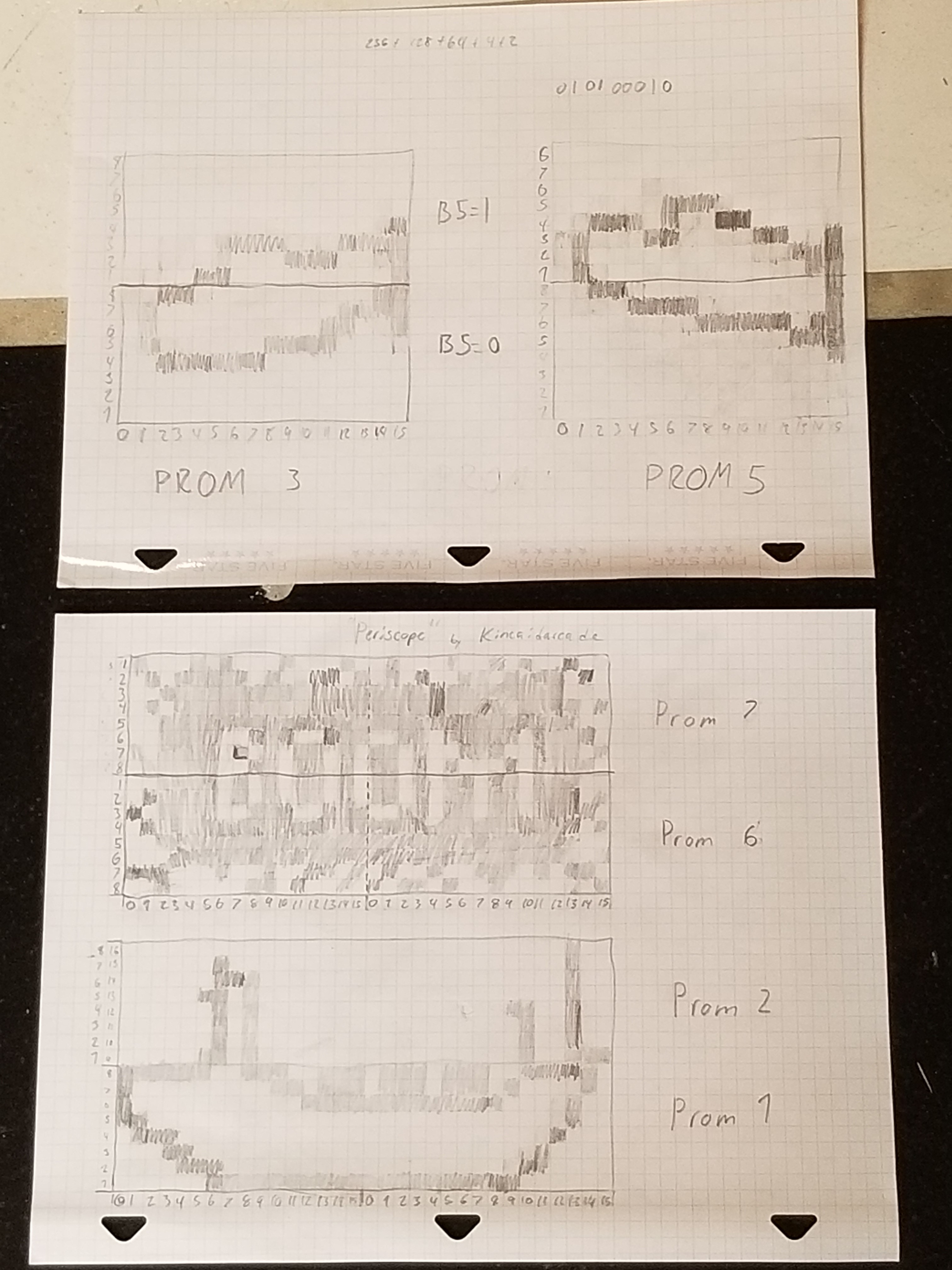
How I Progammed My PROMS:
I decided to use the 82S23 after deciding that using a 2716 would be a little too much hassle for the scope of my project.
I went on EBAY, found 100 PROMS and a programmer, and had my parents buy them.
The programmer was an Ademco Security System programmer. (Which used 82S23s)
The Programmer is the Ademco 690A:
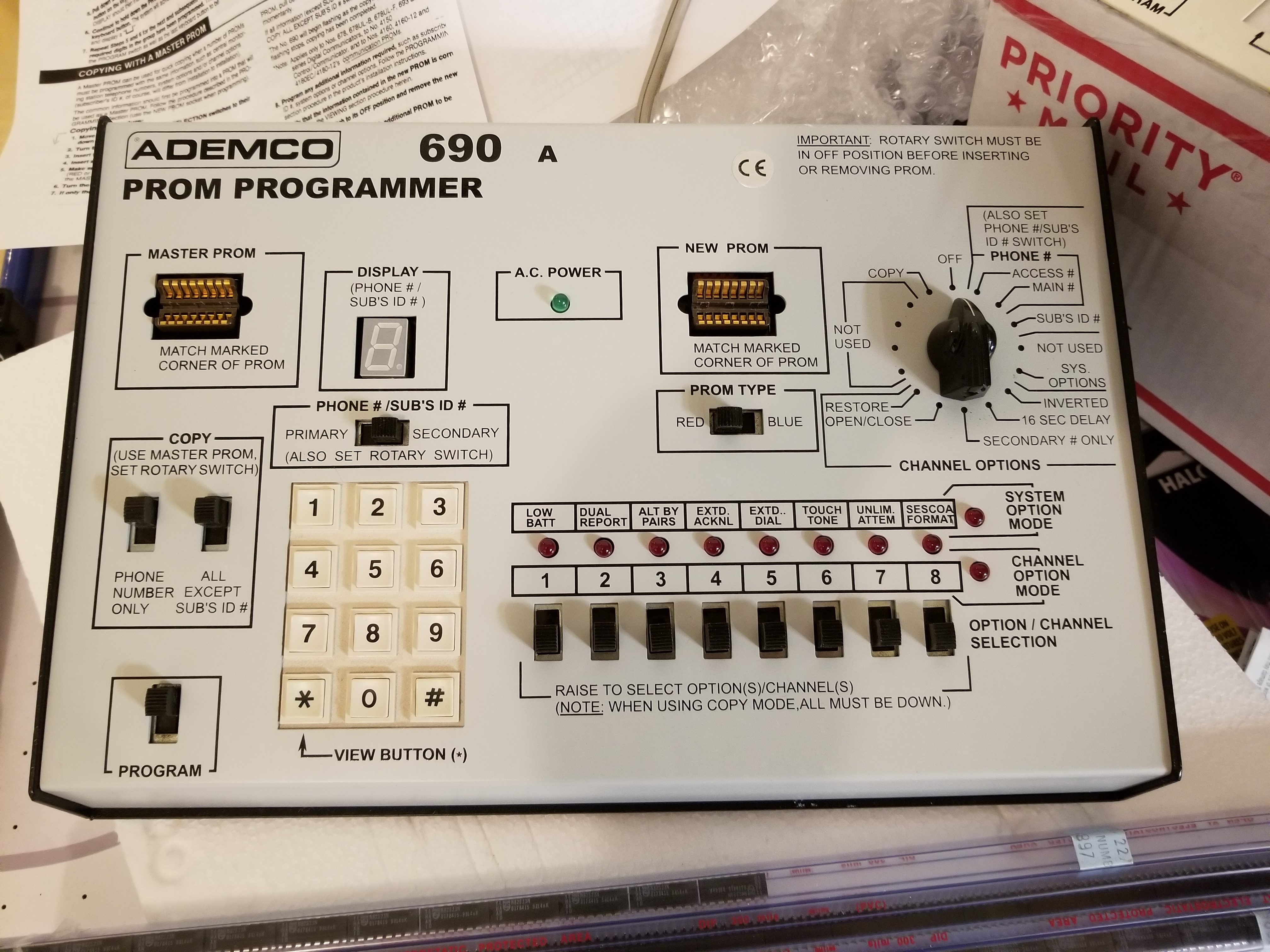
I opened it up later to find a whole bunch of CMOS and TTL chips, with an 82S23 in the center. I found that to be hilarious.
After trying to use it to program my PROMS, I realized that Ademco simplified the user-end of programming their security systems, so I couldn't select memory addresses and data for that address.
Since I couldn't use the refurbished programmer for my specific task, it became obvious that I would need to make my own.
I designed it around the Sigentics Generic 1 Programming Procedures, and around the schematic supplied by this website.
I ended up doing a little redesign to allow it to program 8 bits at a time. (Well, if I need to program 8 of 8 bits in an address, I have to program 4 at a time. Sometimes I can program 7 at once, sometimes I can't. Varies PROM to PROM. I'm guessing it has to do with the current the programmer can supply.)
Here is my programmer:
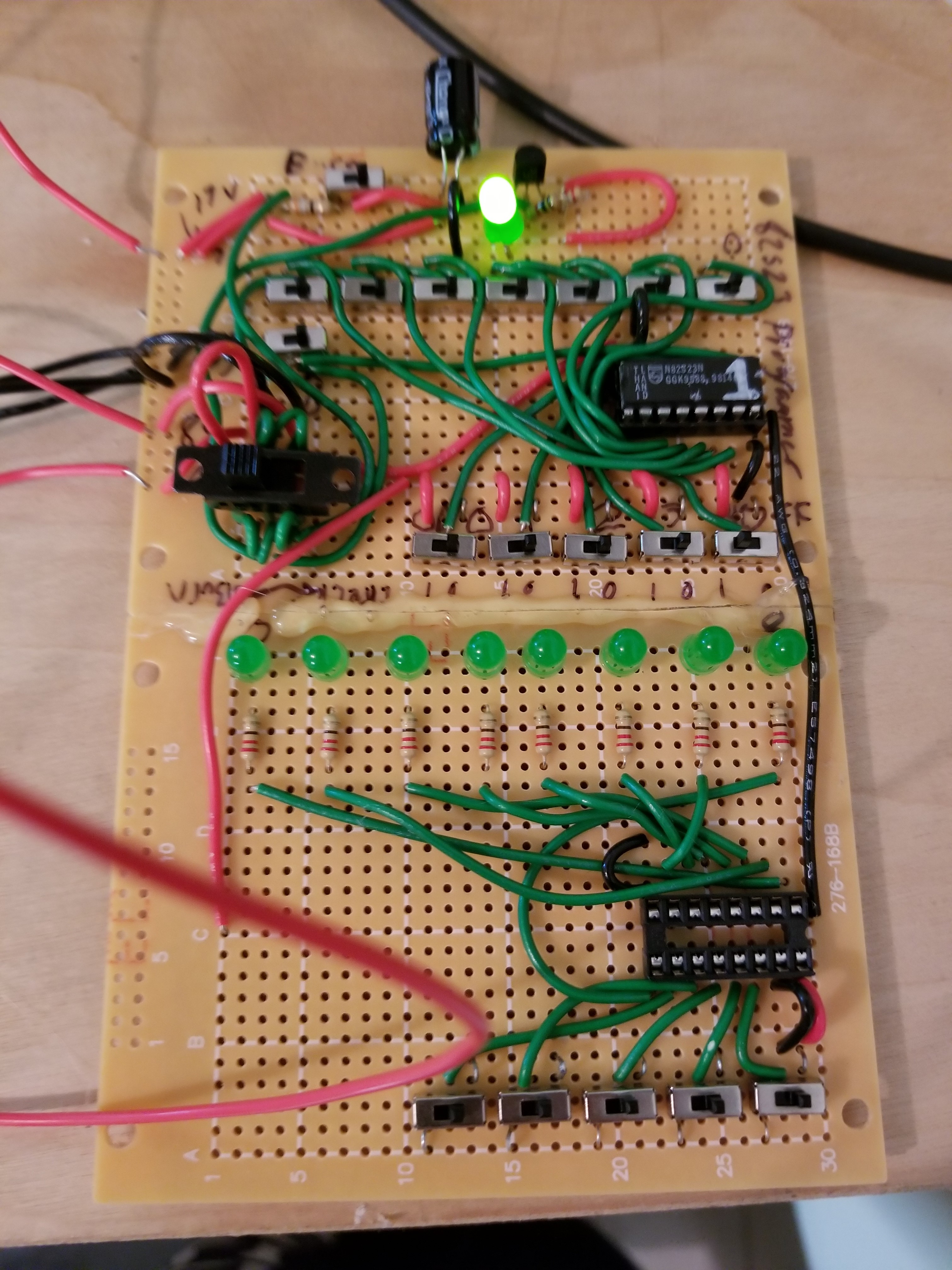
The green light is off if there are bits that don't match the switches. It is on if everything is correct.
For making the PROMS, I just drew everything out on graph paper, marked the addresses, put in a PROM, and would stand there for the next hour or so flipping switches.
Pro Tip: If possible, buy a hundred PROMS or so, you can only program them once, and I can guarentee that you will make mistakes. Of the 100 I got originally, I only have about 50 left.
About 25 were mistakes, and about 25 just weren't aesthetically pleasing so I just ditched them and changed the drawings on the graph paper.
Here are some of the graph papers:
The Submarine Graphics Circuit:
The Submarine Graphics Circuit is located on pages 16 and 17 of the REV-C schematic, and I designed something that only worked for 2 seconds on page 8 of the PROTO-A schematic.
L5, L6, and L7 are 256-bit PROMS that store a 16 x 16 Submarine rotation graphic. (L5: "Up" L6: "Level" L7: "Down")
They take Horizontal Sync Generator signals 1H, 2H, 4H and 8H to select a memory position. Each position stores 8 bits, one bit per vertical line.
Becuase of the way I coded the PROMS, I need to use inverters F8C, D, E, and F to invert SQA, SQB, SQC, and SQD to make sure weird things don't happen to the graphics.
/SQD is used to decide which half of the PROMs at L5, L6 and L7 are being accessed, which chooses whether the top or bottom 8 lines of the graphic are being displayed.
J5, J6, and J7 are data selectors that use Submarine Motion Circuit signals /SQA, /SQB, and /SQC to select which of the 8 lines of data is selected, because the monitor can only display one pixel at a time, not eight.
F7A, B and C and F8A & B take the Submarine Motion Circuit preset signals to determine what direction the motion circuit is counting.
These signals are used to enable the outputs of J5, J6, and J7 to determine which Submarine rotation graphic is displayed.
I6A & C OR together the SUBUP, SUBLEVEL, and SUBDOWN graphic signals, because only one is active at any given time, to become the SUBPROMDATA signal.
I had to use pullup resistors on each PROM because they had open-collector outputs.
After all that work, this is what appeared after I coined it up:
The clicking sounds are the switches in the joystick.
I ended up having to program a new "UP" PROM because I got the halves switched around when I programmed it, even though I could've switched a wire on my prototype to fix it.
Freighter Graphics:
The Freighter Graphics circuit is located on pages 12 and 13 of the REV-C schematic. I designed something that I never tried on page 7 of the PROTO-A schematic.
After having success with the Submarine Graphics circuit, I felt pretty confident about the Freighter Graphics circuit.
The only real difference between the Freighter and Submarine graphics circuits are the use of a pixel counter in the Freighter Graphics circuit.
Because the outputs of the Freighter Motion circuit count by two pixels, (because I put in 1H instead of the Clock signal) the graphics would be stretched by 2 pixels on the horizontal axis, and only 16 pixels of space would be reached. I decided that wasn't good enough for my game. I needed something better.
One of the first things I designed was the pixel counter.
The pixel counter is composed of counters I3 and I4. The counters count during the duration of the Freighter's H position, and are in a clear state the rest of the time.
They take the Clock signal and divide it into FQA, FQB, FQC, FQD, and FQE.
I can't just use 1H, 2H, 4H, 8H, and 16H because then the Freighter graphic would have parts drawn out of order if the Freighter's H position doesn't start when 1H, 2H, 4H, 8H, and 16H are all equal to 0. Which only happens 1 out of 32 times.
FQA, FQB, FQC, FQD, and FQE are fed into the inputs on PROMS L3, L4, L8, and L9.
J3, J4, J8, and J9 are data selectors, which use /1V, /2V, /4V, to select which line is being displayed. 8V and /8V are used to enable the outputs of each of these data selectors, which also selects whether the top or bottom PROM's data makes it to the next stage.
D5A and D5B then OR the outputs of the data selectors for PROMS 1 & 2 and 6 & 7. (Each group only has one active data selector output at a time.)
I5C and I5D are used to determine which graphic is selected. If an explosion is active, the group with PROMS 6 & 7 is selected. If there is no explosion in progress, then the group with PROMS 1 and 2 is selected.
The outputs are then fed into an OR gate at D5C, which allows each signal to become the FREIGHTERPROMDATA when it is their turns.
After soldering up too many wires, this is what appeared:
I had a switch soldered in to simulate the Torpedo, which I hadn't added yet. You can just barely hear me flipping the switch.
This was also before I added B4C to the Freighter Control circuit to make the Freighter (seem to) instantly reappear at the left of the screen.
And here is the circuit board:

If you look close enough, you can see the PROMS. They can be identified by the white numbers I put on the top with a paint pen.
Each PROM has 256 bits of memory, and there are 7 PROMS. That means there is 1,792 bits of memory on the board. (Technically 1.75 Kilobits)
You can also see evidence of circuits I abandoned. They can be identified by the empty sockets.
The Torpedo Motion Circuits:
The Torpedo Motion circuit is on page 18 of the REV-C schematic. I also designed something that certainly wouldn't have worked on page 10 of the PROTO-A schematic.
Okay, breathe Me-Of-The-Past. It's finally time to stop putting off what you've been dreading: The Torpedo circuit. For the Torpedo Motion Circuit, I copied the counters from the Ball in PONG. The control circuits are completely different. Wait. I just realized the implications of this: I have just turned a video ping-pong ball into a highly leathal anti-ship weapon.
The Vertical Torpedo Motion circuit in PONG and PERISCOPE is a typical Atari vertical motion circuit, with a 3-input NAND (G5A) and an inverter (D8A) added to the circuit. [G5A] takes where the normal 16-pixel output would be found, (Pin 15, F6,) and NANDS it with outputs C and D from the first counter. Outputs C and D are only both active for a period of 4 pixels of the 16 pixels that makes the vertical window. That is how we get a 4-pixel window. If you wanted an 8 pixel window, only use output D, (and change to a 2-input NAND) if you wanted a 2 pixel window, use outputs B, C and D. (And change to a 4-input NAND) If you wanted a 1-pixel window, use all four outputs. (A, B, C, and D, and change to a 5-input NAND). All of this is then inverted by D8A to create the output "Torpedo". Also: Feel free at any point to change the n-input NAND and an inverter to a n-input AND with no inverter.
The Horizontal Torpedo Motion circuit in PONG and PERISCOPE is a typical Atari horizontal motion circuit. The only change is that it has 4-input AND at H5A.
The 4-input AND at H5A uses outputs B and C of G6. Outputs B and C are only active for 4 pixels of the 16 pixels that makes the horizontal window. The other two inputs are used for creating the 16 pixel horizontal window, which it ANDs with the 4 pixel window, and that is how you get a 4-pixel horizontal window. Make the changes as mentioned above, and you can vary the width of your windows. If you got crazy with some extra ANDs and ORs, you could make 3, 5,6,7, etc. pixel windows.
In order to show the Torpedo on the screen at this stage, you need one additional piece of circuitry.
H5B is a 4-input AND, that has had one of its pins tied to a pullup resistor, turning it into a 3-input AND.
It takes the Horizontal and Vertical windows and makes a 4 x 4 pixel square. Before outputting it, it adds the VISBLETORPEDO signal.
The VISIBLETORPEDO signal determines whether or not the Torpedo gets drawn on the screen.
This is where we get our Torpedo. However, if you turned it on at this stage, the Torpedo would be moving at lightspeed. Why? Because the Motion circuits don't have control circuits yet.
The Torpedo Control Circuits:
The Torpedo Control Circuit is located on pages 18 and 19 of the REV-C schematic. I designed something that wouldn't have worked on page 10 of the PROTO-A schematic.
I designed the Torpedo Control circuit myself. It is by far the most complicated circuit in PERISCOPE.
The only part of it that is on page 18 of the REV-C schematic is the part that governs when the Torpedo can be fired.
The input "FIRE" comes into the board. It is pulled up by a 1K resistor, and is fed into a NOT gate, A.K.A. an inverter, D8B, to have the output be "0" when it is not pressed. If I used a normally closed switch, I would've needed to remove D8B.
The 4-input AND gate at H4B checks if:
- The start button has been pressed, AND
- A game is in progress, AND
- The Torpedo is invisible/not active, AND
- The Torpedo has already been centered.
If all those conditions are true, the signal JUSTSHOT becomes a "1" (5 volts), and we move to the next page, page 19.
The signal JUSTSHOT is sent into the Torpedo Movement Lock circuit.
The Torpedo Movement Lock circuit is composed of two 2 flip-flops at I7A & B, 2 AND gates at I5A & B, and 2 OR gates at I6B & D. It is used to lock in the vertical Torpedo movement, so you can't control your Torpedo like in Computer Space.
When the Torpedo is JUSTSHOT, the flip-flops at I7 lock in the Presets from the Submarine Motion circuit. They are then passed through the OR gates at I6B and I6D.
The OR gates allow the other option of the Torpedo to move up and down if it is in the Submarine. That is determined by the AND gates at I5A & B.
When the Torpedo hits something, the flip-flops at I7 reset, and the repositioning circuits move the Torpedo back into the Submarine.
The HITS circuit at the bottom left of page 19 determines all the possible collisons the Torpedo can have.
G7B and F9C & D are AND gates. G7B checks if the Torpedo has hit the ocean. F9D checks if the Torpedo has hit the STARTLINE. F9C Checks if the Torpedo has hit 256V (the bottom of the screen).
All of these conditions plus the one on page 11 of the REV-C schematic that is determined by A7B are ORed together by E8A,B, and C.
All of this makes the Signal HITS go high when the Torpedo hits something.
To satisfy the inverted clears of the different flip-flops on the board, the NOT gate at D8E inverts it.
The Visible Torpedo circuit keeps track of whether or not the Torpedo is visible.
The Visible Torpedo circuit starts with the AND gate of G7A, which is actually unnecessary. It's function is already accomplished by H4B, which creates the JUSTSHOT signal. Anyway, It keeps the Torpedo from being shot if it isn't ready to be shot. If it is ready to be shot, it toggles the Flip-Flop at E7B, which makes the Torpedo visible. When the Torpedo hits something, the flip-flop at E7B is cleared by /Hits, and the Torpedo goes to be re-centered.
The Torpedo's horizontal speed and movement is determined by the Torpedo Horizontal Motion Circuit Preset Circuit. (These names are getting too elaborate...)
The Torpedo Horizontal Motion Circuit Preset Circuit (which I will just refer to as the THMCPC) is comprised of the 3-input NAND gate at G5C, a NOT gate at D8C, and an OR gate at E8D.
I wanted to have the Torpedo move faster than when I used VRESET as the speed, (VBLANK was way too fast...), so I used G5C and D8C to create a signal that is active for longer than a VRESET.
The OR gate at E8D allows the Torpedo to move at lightspeed if it needs to bee moved to the center of the Submarine. That is determined by the signal MOVETORPEDOH.
The Torpedo Horizontal Reposition circuit is located at the bottom right of schematic page 19.
It consists of two AND gates, at F9B and G7D, and a flip-flop, at G8B.
When the Torpedo /HITS something, G8B is reset and the signal MOVETORPEDOH goes high.
When the torpedo hits the back end of the Submarine, as determined by F9B and G7D, (Hmm... I could remove a gate from that circuit, too) it toggles the flip-flop, and the TORPEDOHCORRECT signal goes HIGH, indicating that the Torpedo has centered itself in the Submarine on the X-Axis.
The Torpedo Vertical Reposition Circuit is located in the middle right of page 19.
I think I can improve this circuit...
This circuit is a little more complex than the Torpedo Horizontal Reposition Circuit.
It consists of a flip-flop at G8A, an AND gate at G7C, a NOT gate at D8D, and a 8-input NAND gate at H7.
When the Torpedo /HITS something, it resets G8A, signaling that the Torpedo's vertical position is incorrect.
The 8-input NAND gate at H7 has been changed to a 5-input NAND gate by having 3 of its inputs connected to a pullup resistor.
When combined with the NOT gate at D8D, it becomes the equivalent of a 5-input AND gate.
It checks if the game still thinks the Torpedo's position is incorrect, and the Torpedo has hit the center of the SUB. (Line 10 to be exact. Defined by SQB and SQD.)
By the way: Re-Evaluating my logic makes me think that the MOVEDOWN signal needs to be renamed to TORPEDOVNOWCORRECT. (Torpedo V Now Correct)
If /MOVEDOWN and TORPEDOHCORRECT are both True, then the flip-flop at G8A toggles, and it tells the game the Torpedo's V is correct.
The game knows the torpedo is centered when F9A's output CENTERED is HIGH.
F9A outputs CENTERED if TORPEDOVCORRECT AND TORPEDOHCORRECT is true.
And that, Ladies and Gentelmen, is how you make a Torpedo Control circuit.
After soldering all that up and going through 20 iterations of the circuit before getting what I just described, this is what appeared:
YEEEEEEEEEEEEEAAAAAAAAAAAAAAH!
After I stopped screaming for joy, I took a picture of the prototype:
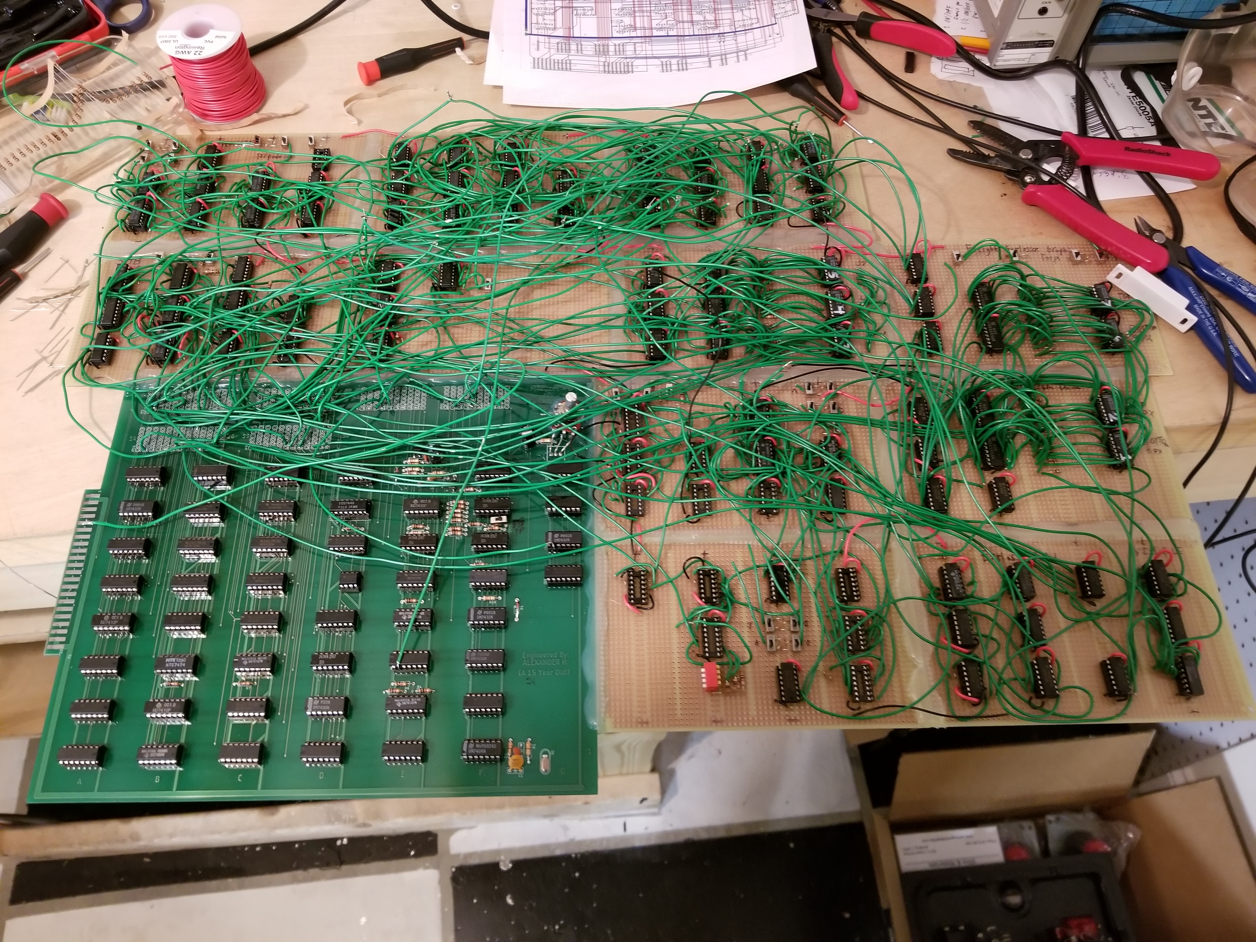
That thing is huge!
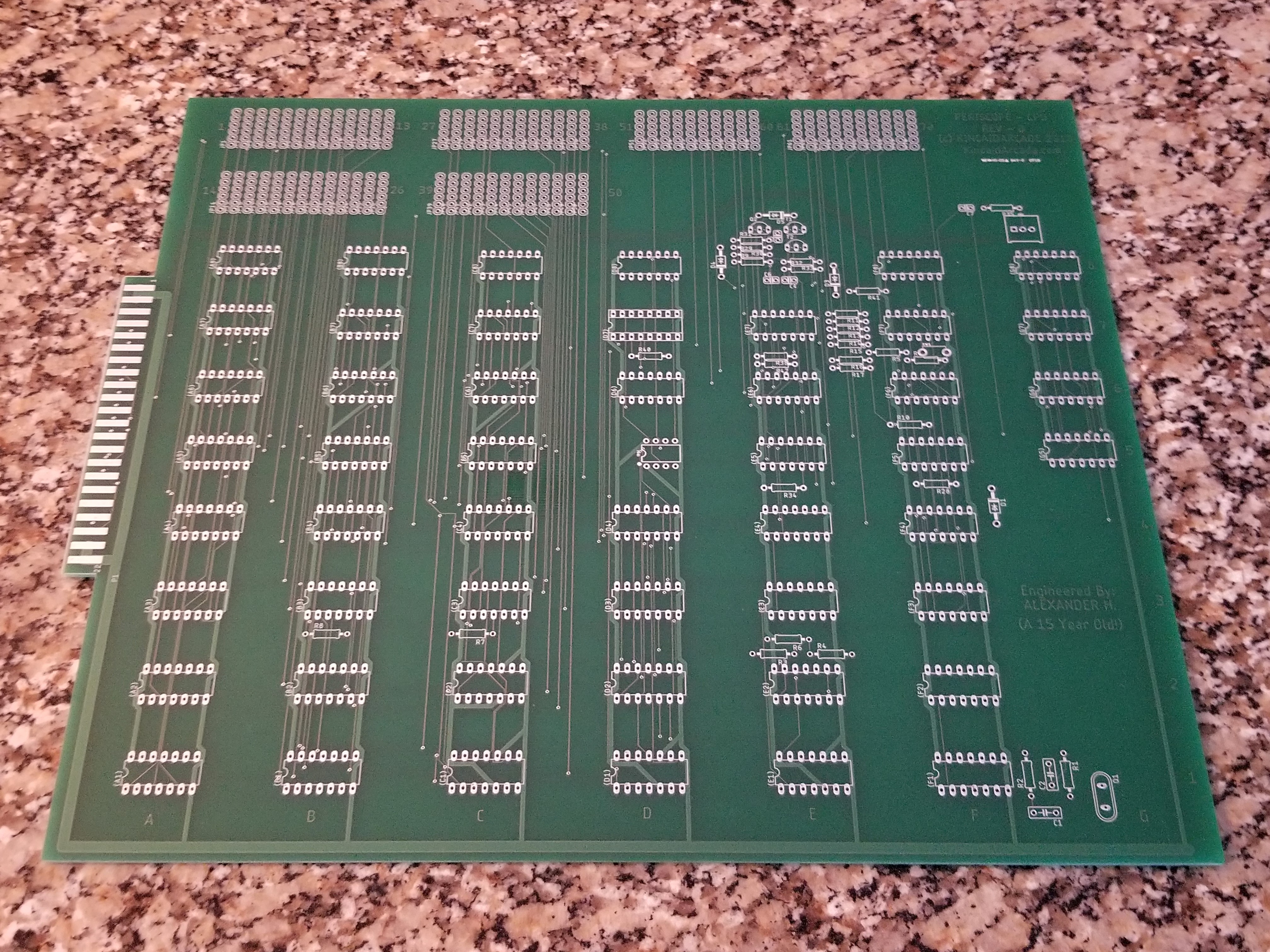
Designing The OBJ Board:
I now had this ginormous prototype, and with all the wires it had, it was easy to tell that it wouldn't work much longer. So, the next logical choice was to design another board. I decided to call it the OBJ (object) board because it handled the Submarine, Freighter, and Torpedo. Using the schematic I was working on, I created a board, and had Quick Turn PCB fabricate it for me.
Again, really pleased with the results:
After soldering up a new board and an old board, and adding wires to interconnect them, this was the product:
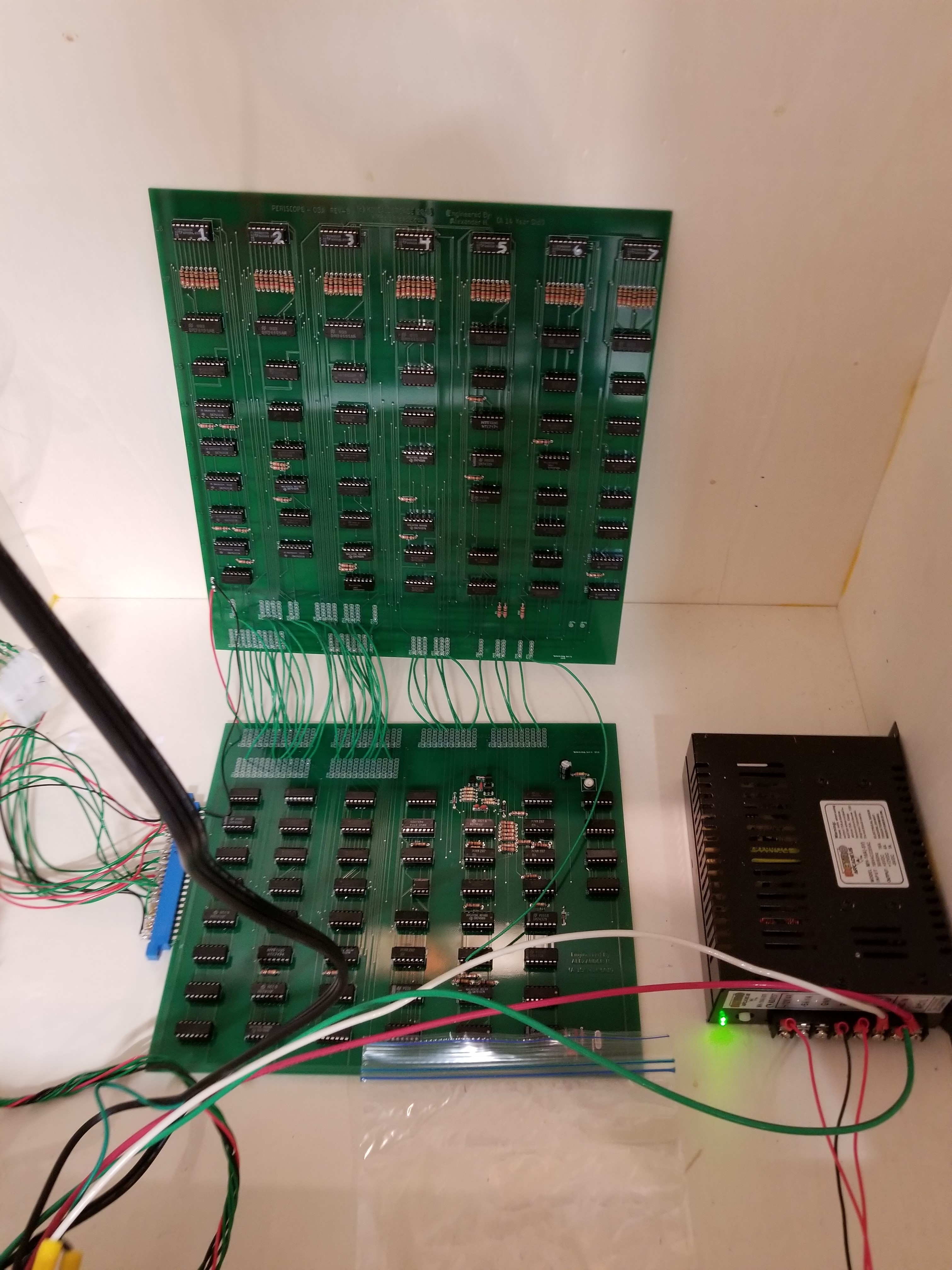
And then, I found out that there were errors:
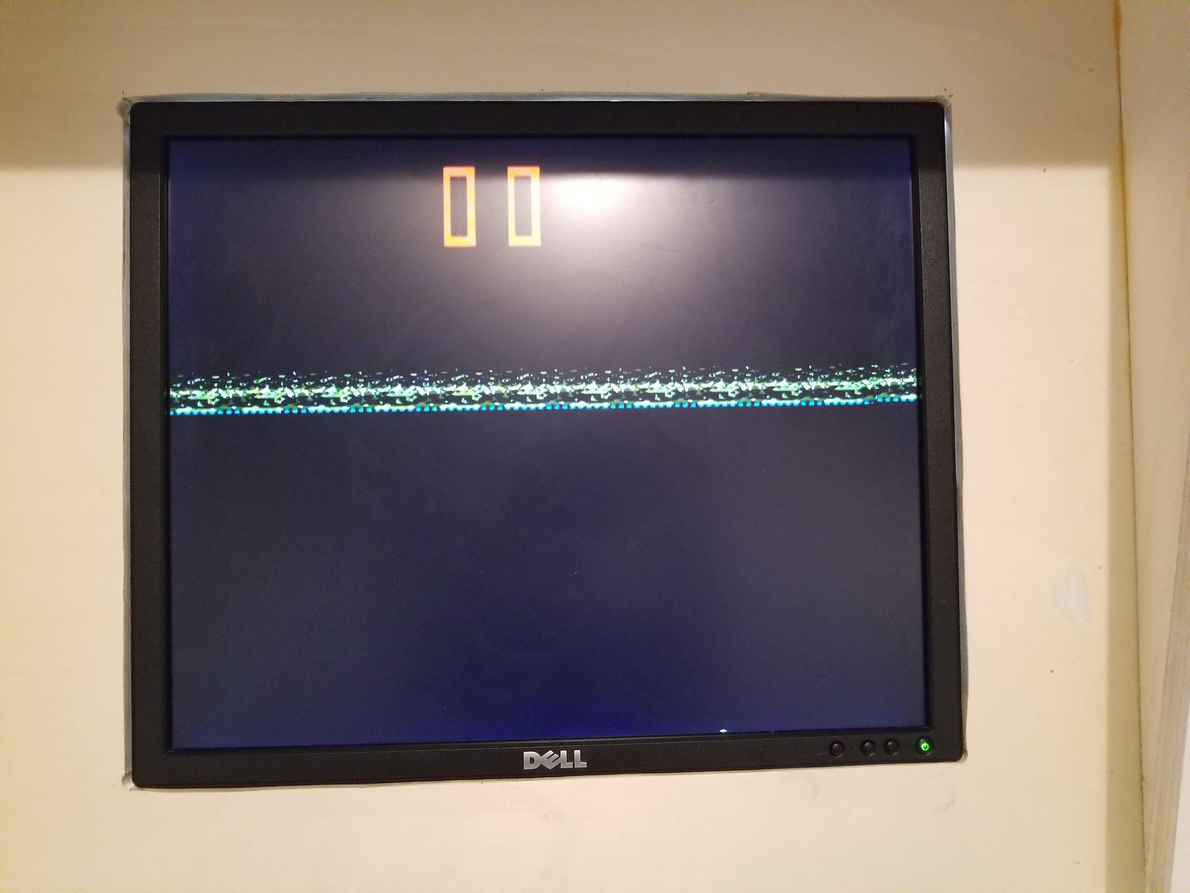
Well, looks like I need to cut and jumper some traces...
One of the things I'm wondering after the fact is how the submarine got stuck in vertical blanking. (You can see the top couple pixels of the Submarine at the bottom of the screen.) When something like this happens, you should re-evalulate your circuit logic and check your work. When doing this, I made a list of modifications to the OBJ board:
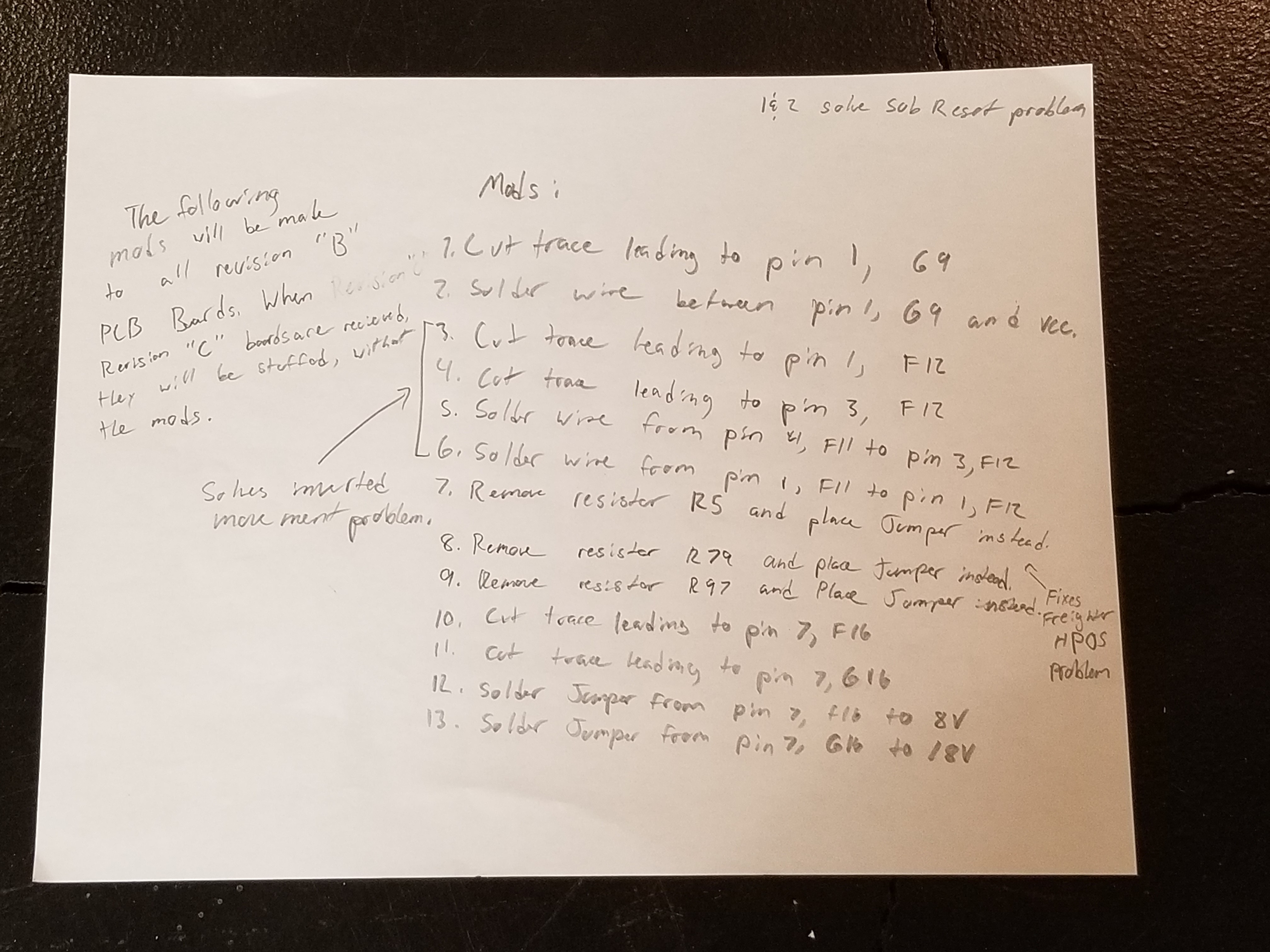
- Cut trace leading to pin 1, G9
- Solder wire between pin 1, G9 and VCC (+5 volts)
- Cut trace leading to pin 1, F12
- Cut trace leading to pin 3, F12
- Solder wire from pin 4, F11 to pin 3, F12
- Solder wire from pin 1, F11 to pin 1, F12
- Remove resistor R5 and place jumper instead
- Remove Resistor R79 and place jumper instead
- Remove Resistor R97 and place jumper instead
- Cut trace leading to pin 7, F16
- Cut trace leading to pin 7, G16
- Solder jumper from pin 7, F16 to 8V
- Solder jumper from pin 7, G16 to /8V
All of the mods I had to make were because I missed several errors in my schematic when checking my work...
All of the resistors I had to remove were because apparently I left resistors between pins and ground, rather than just connecting them to ground. I didn't do this on my working prototype. (Well, I did, but I removed them...)
Mods 1 & 2 fix a problem where the Submarine would reset its position when I hit the start button. (A feature I chose to remove awhile back.)
Mods 3 - 6 fix the Submarine moving in the wrong direction when using the joystick. It would also collide with the bottom and the top wrong with this problem.
Mods 7 - 9 remove pulldown resistors that should've just had all their connected pins connected to ground.
Mods 10 - 13 fix a problem where the BOOM graphic had its top and bottom halves transposed.
The lesson I learned from this: check your work more than once.
Here are all the mods on the board:
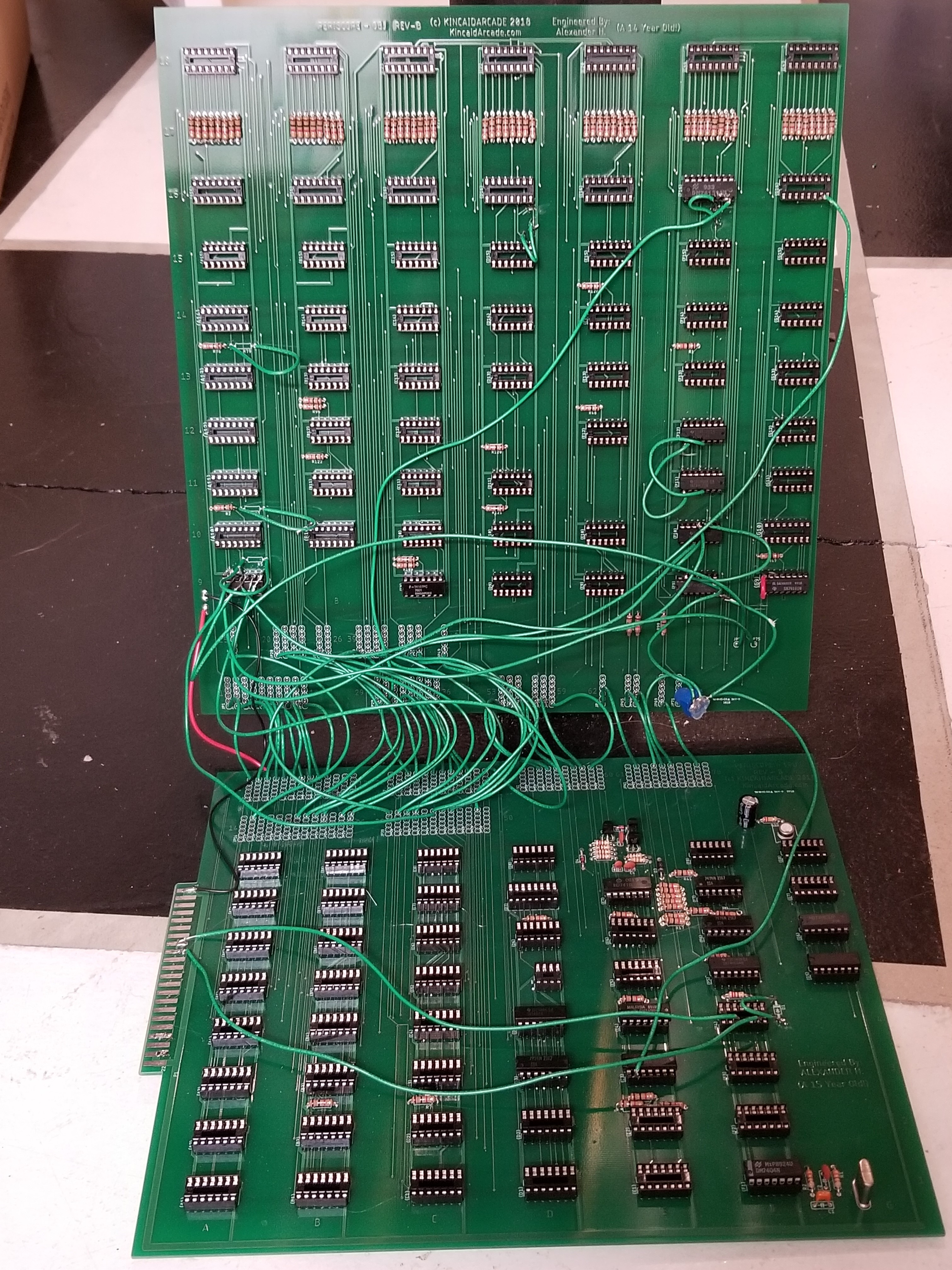
(All the chips are removed because I took the picture after the fact.)
Designing Sound For PERISCOPE:
Before I designed and sent off the OBJ board, I tried to make some sound for PERISCOPE. Due to a time crunch, I had to design the sound separate from the OBJ board.
I had envisioned some BOOM effects and a wooshing torpedo.
Where would I get a BOOM sound and a Thrust sound?
The answer was staring me in the face: Computer Space.
I tried cloning the sound circuit, but to no avail. It never did anything useful... Maybe I needed to use a center-tapped coil?
Well, I guess I'll never know...
Here is the board I tried cloning the Computer Space sound on:
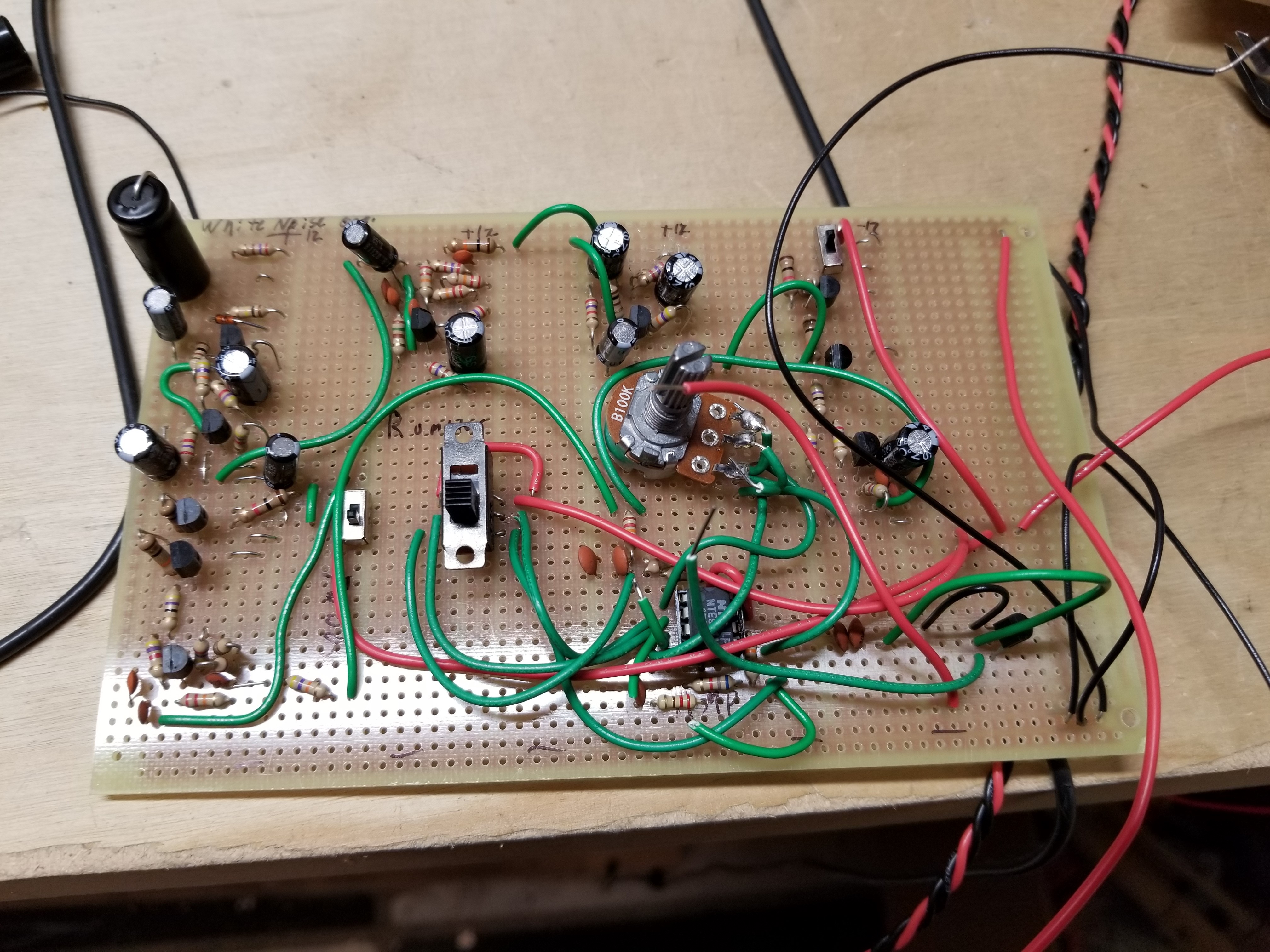
In the end, I chose to just take signals from the Sync Generators that sounded good to make the sound.
The sounds that I chose in the end are located on page 5 of the REV-C schematic.
The sound circuit consists of 2 AND gates at D4A & B, an OR gate at D5D, and a potentiometor to control the volume of the game.
The Torpedo sound is the signal VSYNC (I liked the dull buzz), which is ANDed with the VISBLETORPEDO signal, which enables the Torpedo Buzz.
The BOOM sound is a sound similar to PONG. (Err... I thought I chose something different, but apparently the BOOM sound is the same as the Score sound for PONG, 32V.)
It is then ANDed with the signal ACTIVEEXPLOSION to enable the Boom sound.
Both of these sounds are passed through the OR gate (D5D) which allows both sounds to be output to one speaker. (By combining them if they are both on.)
Lastly, the sounds go through a potentiometor to adjust the volume.
Now that I think about it, I probably could've stuck in a transistor to amplify it... oh well.
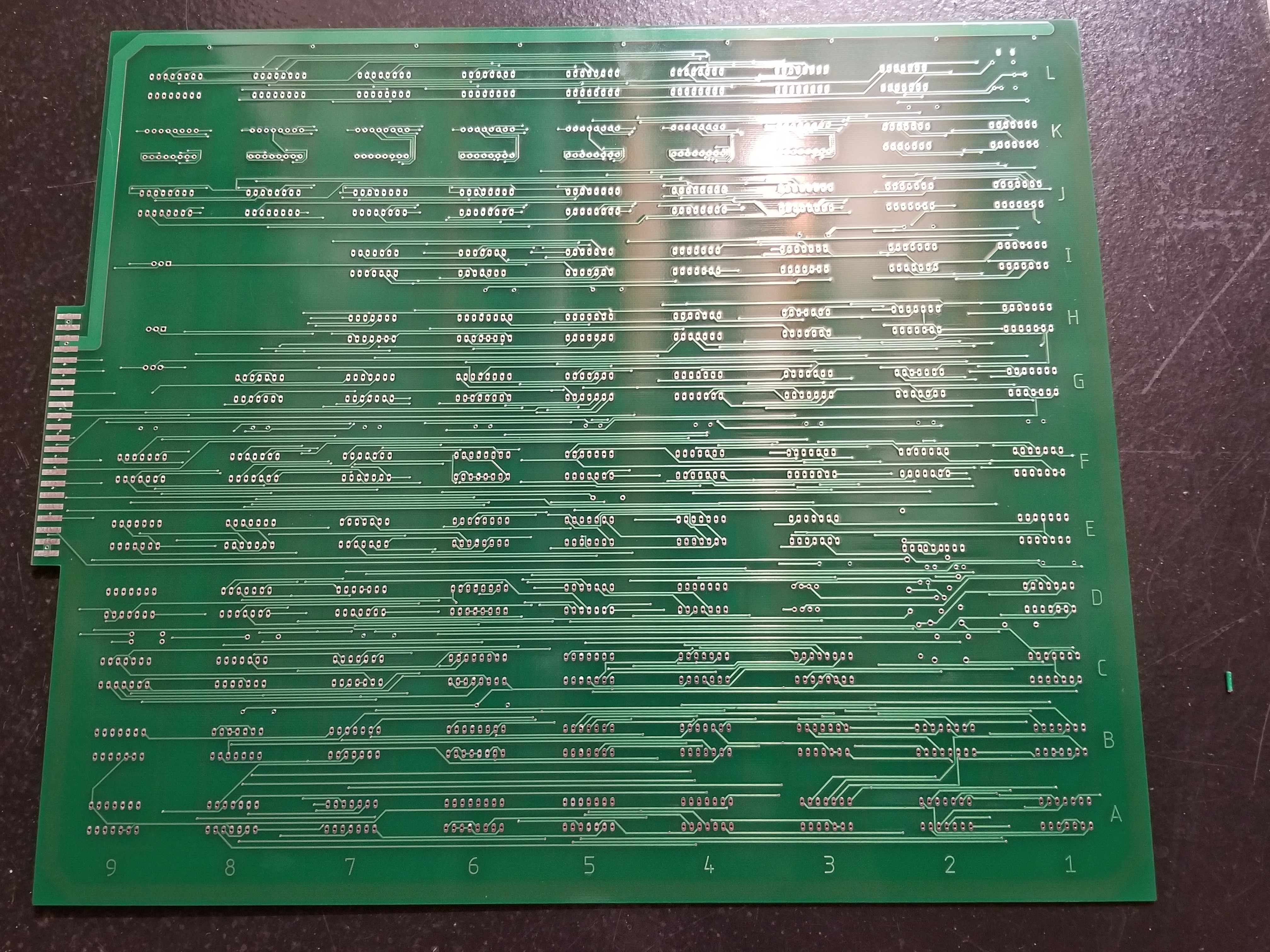
Designing the REV-C Board:
Although I technically had something I could've used for forever, I decided to ditch the board with all the mods. I also wanted to be able to show off that prototype boardset at the Eden Exposition, so I would need some other board in the cabinet I therefore designed the REV-C board in Eagle. I checked my work several times a day, for a little more than a week, re-evaluating EVERY circuit to make sure there were no errors when it arrived.
I ordered it up. I was very excited!
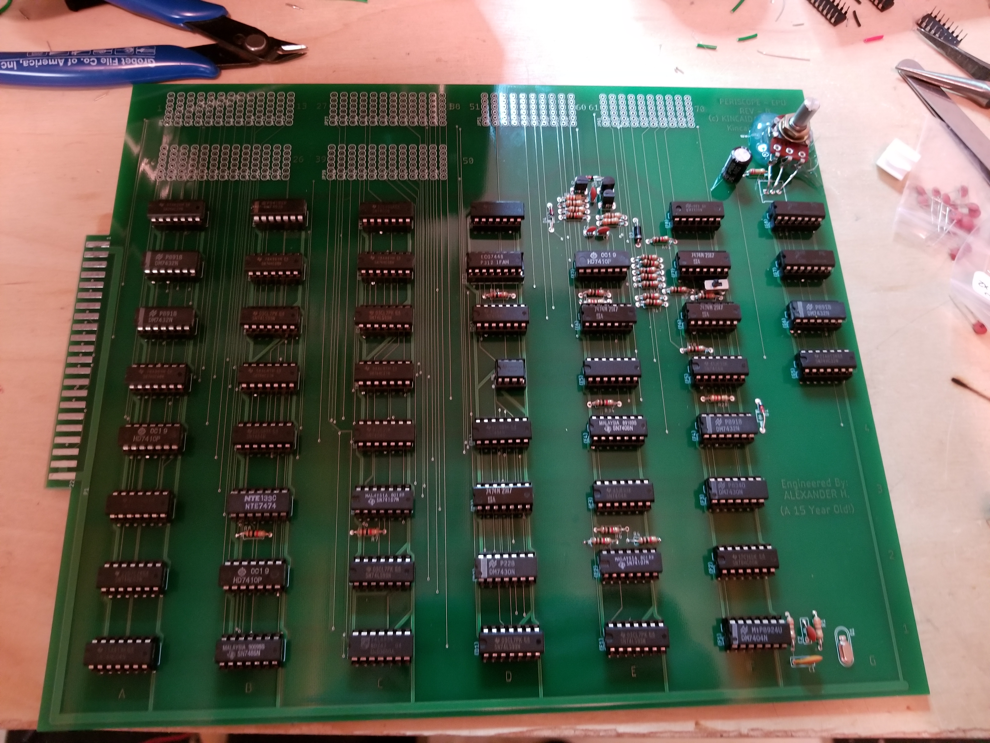
Here is one of the boards that arrived:
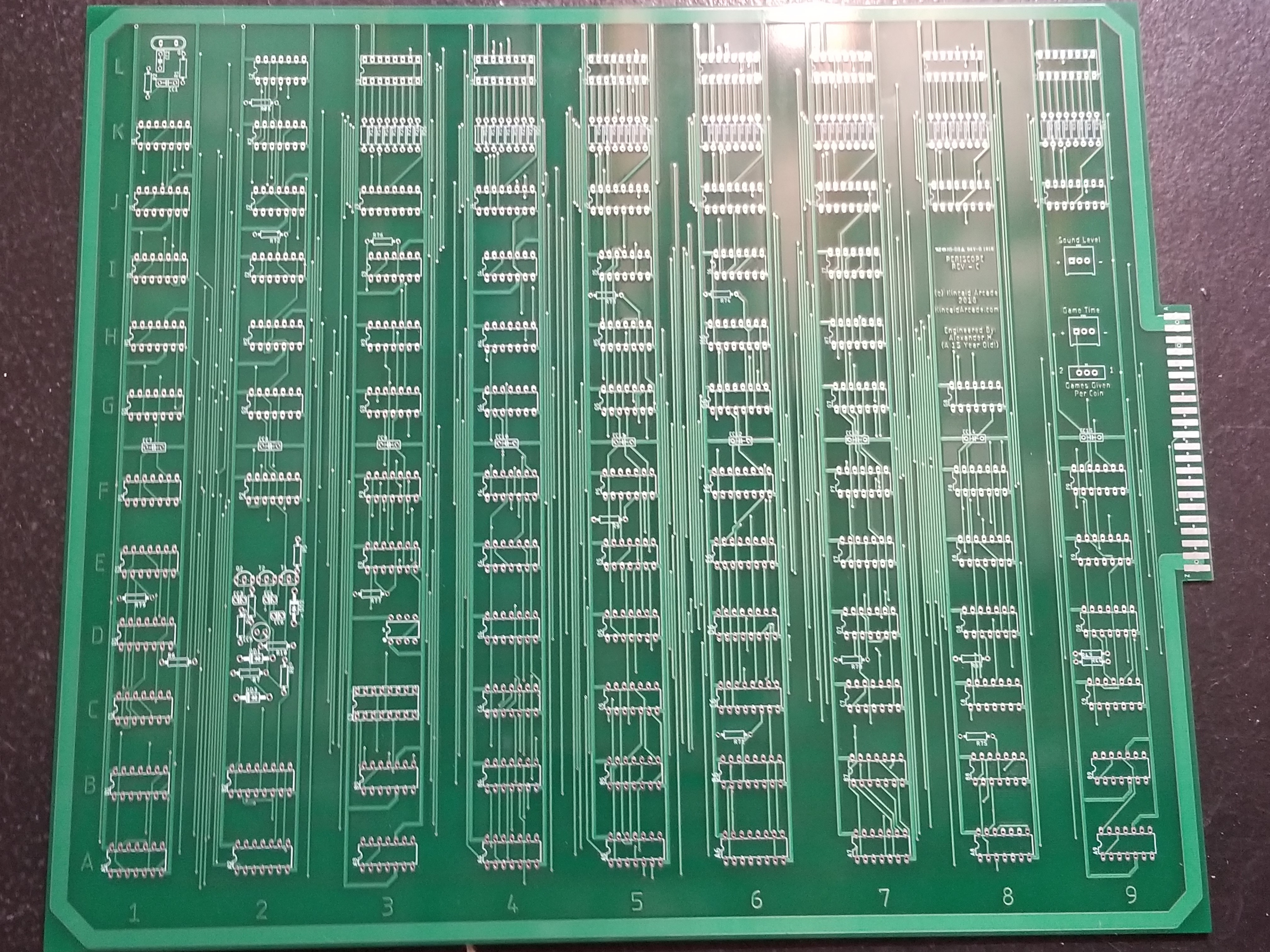
I made sure to credit myself. :)

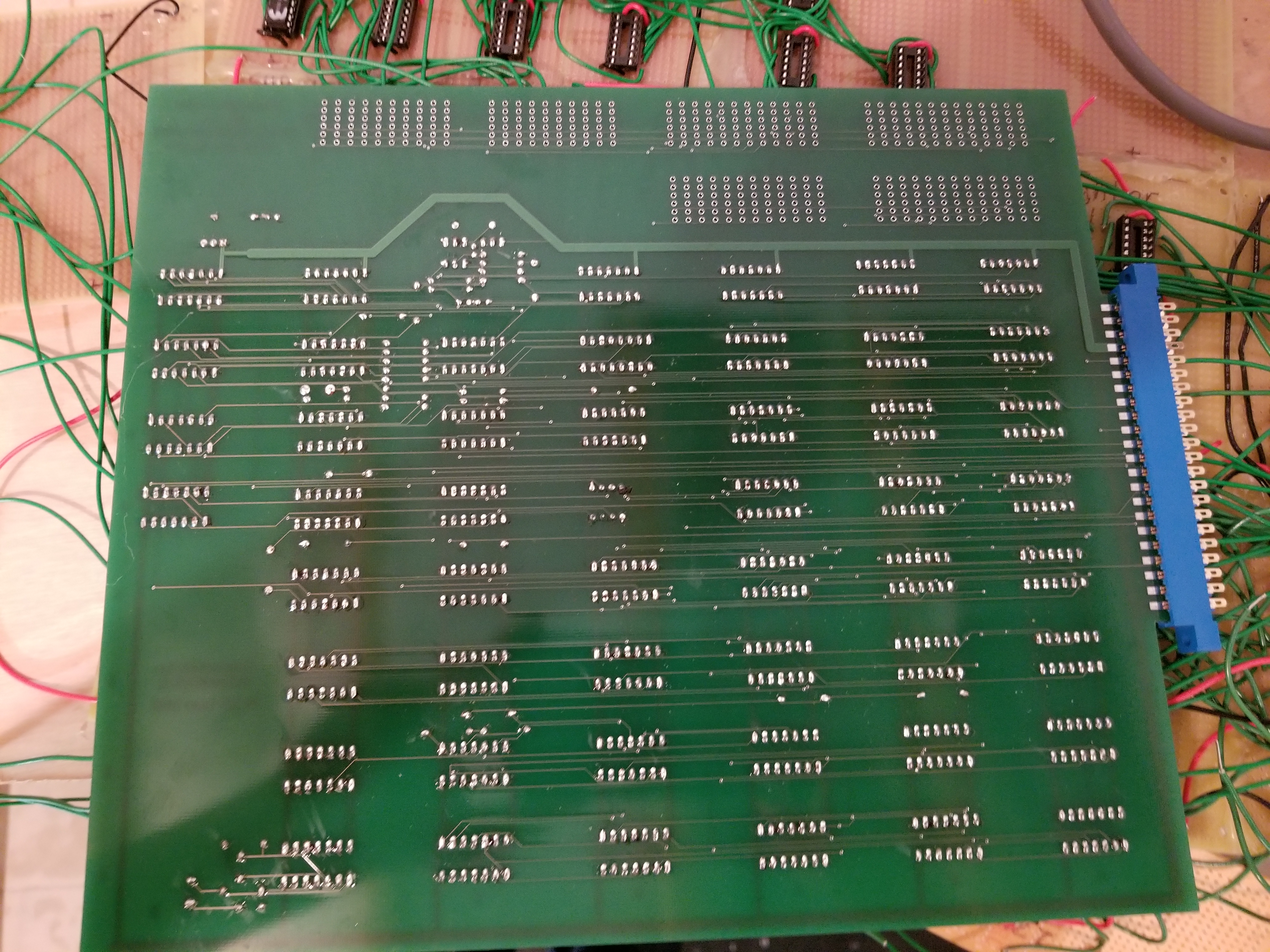
I actually used thick solder meant for pipes (but the same as the electroninc stuff) on the boards. You can't tell from looking at the bottoms, at any angle:
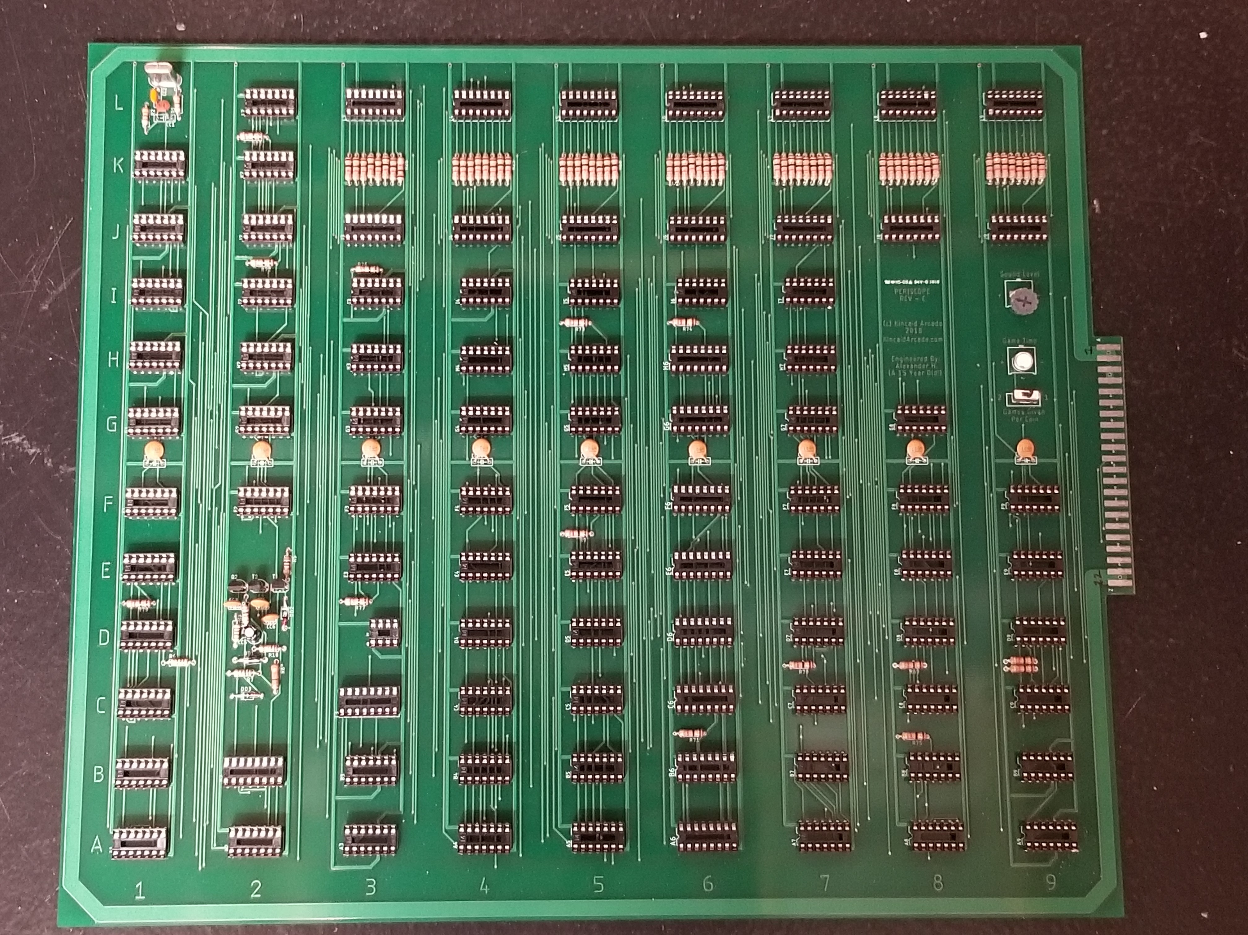

I am pretty good at soldering, even if I do say so myself. :)
I later had to solder up another board. The previous one had a graphical glitch that I couldn't fix in time for the Expo.
This one had a different graphical glitch, too, but it is a little less noticeable.

I later realized that 82S23s apparently don't need external pullups. That is why I left some resistor banks unsoldered. If only I knew that ahead of time...
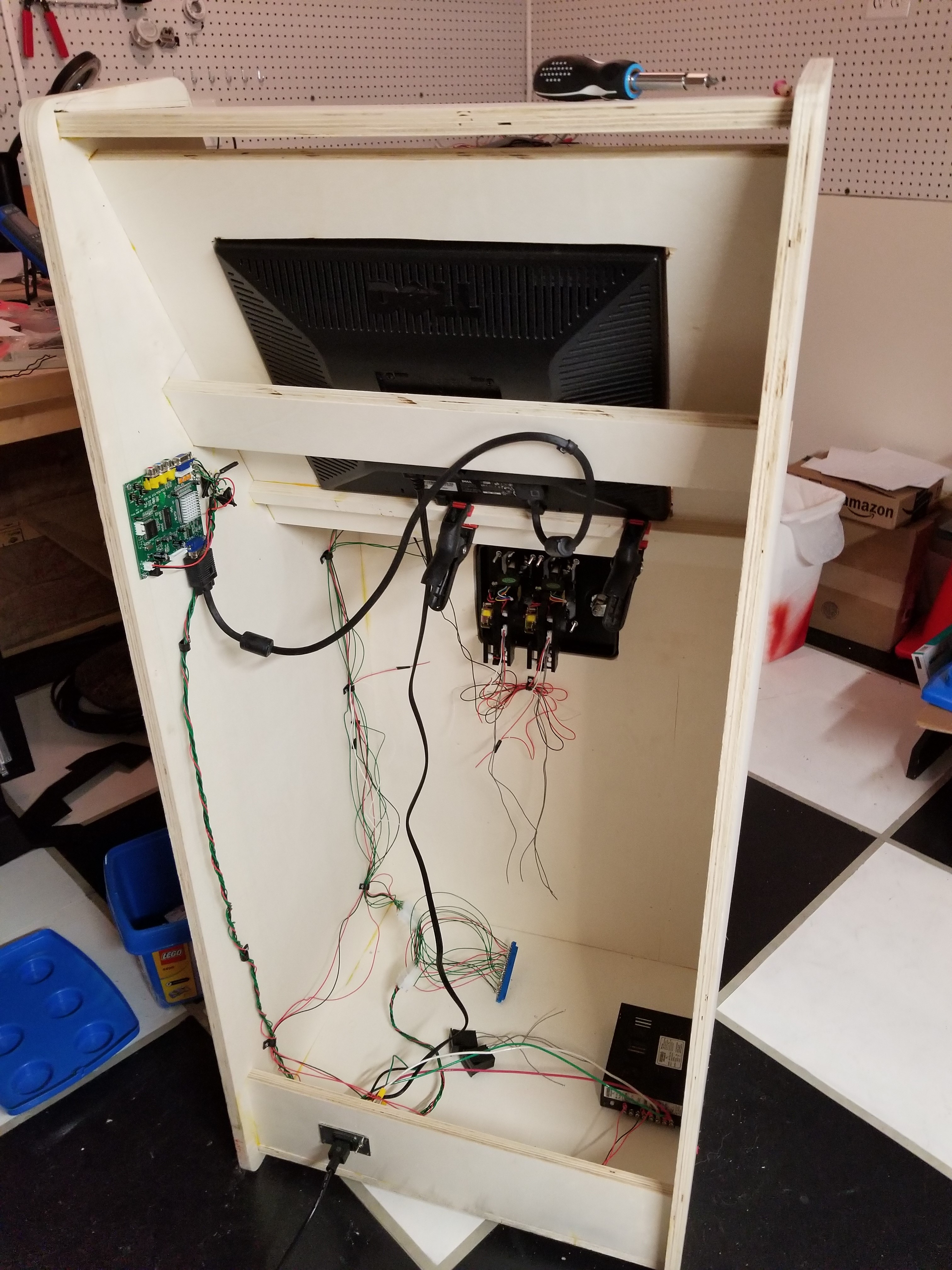
Designing The Cabinet:
First off, the cabinet does look like a Tank II. I actually designed it myself, and I did not butcher a Tank II to make PERISCOPE. I kinda realized that it looked like a Tank II a little too late.
The process of me designing and building the cabinet was spread over almost all the circuits I designed. For the sake of reading, I have consolidated it all here.
The first part of building the cabinet was designing it. I chose to model mine in Rhino 5.
I drafted several designs. One looked like Steeplechase, one looked original, and one (later) looked like Tank II.
Unfortunately, I can't seem to find the file, so I can't put a picture here. Sorry.
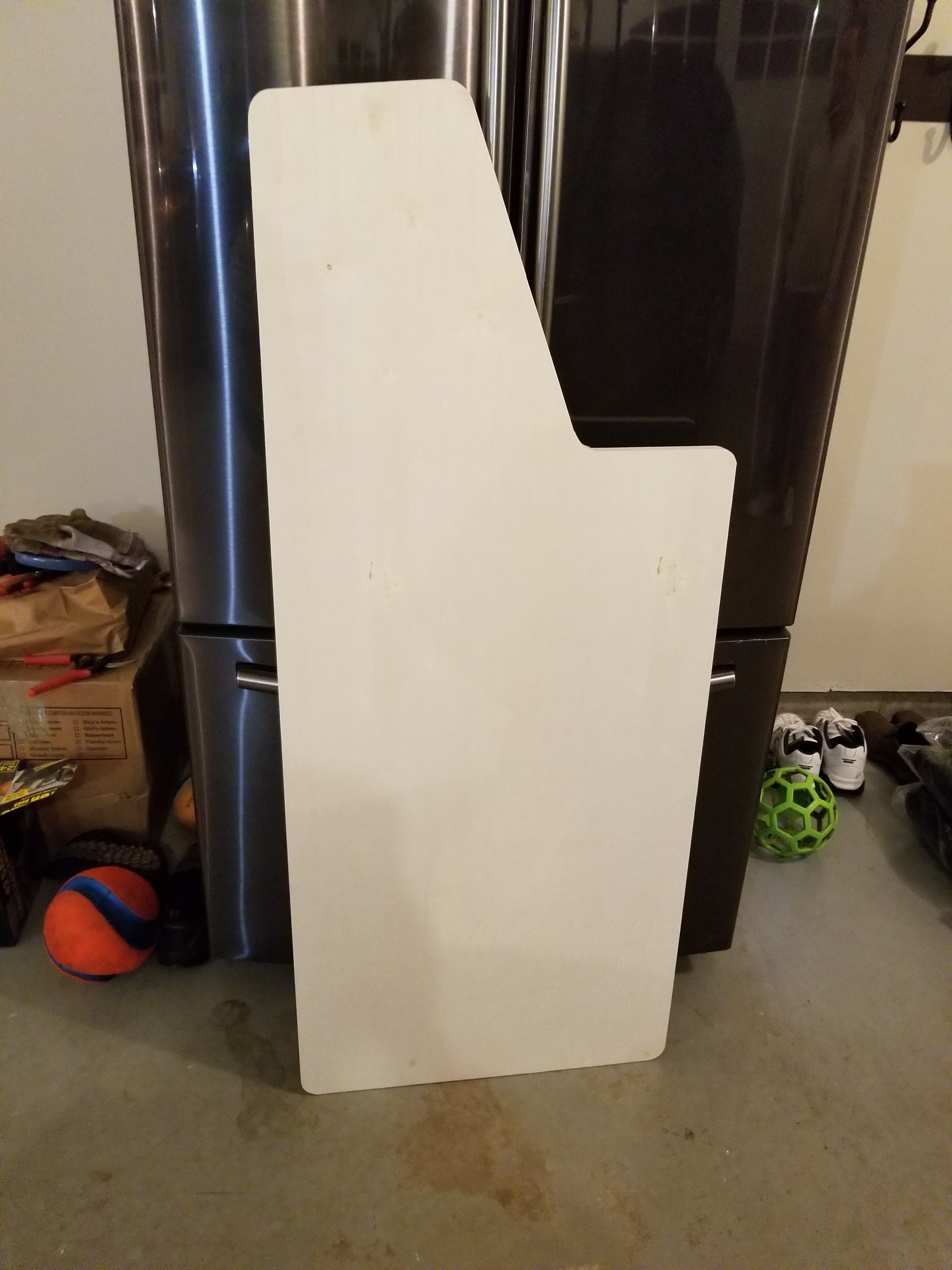
We then made note of the sizes of wood, and we bought some whitewood poplar plywood. That stuff is the bomb.
Here is some of the poplar, with an already-cut side.
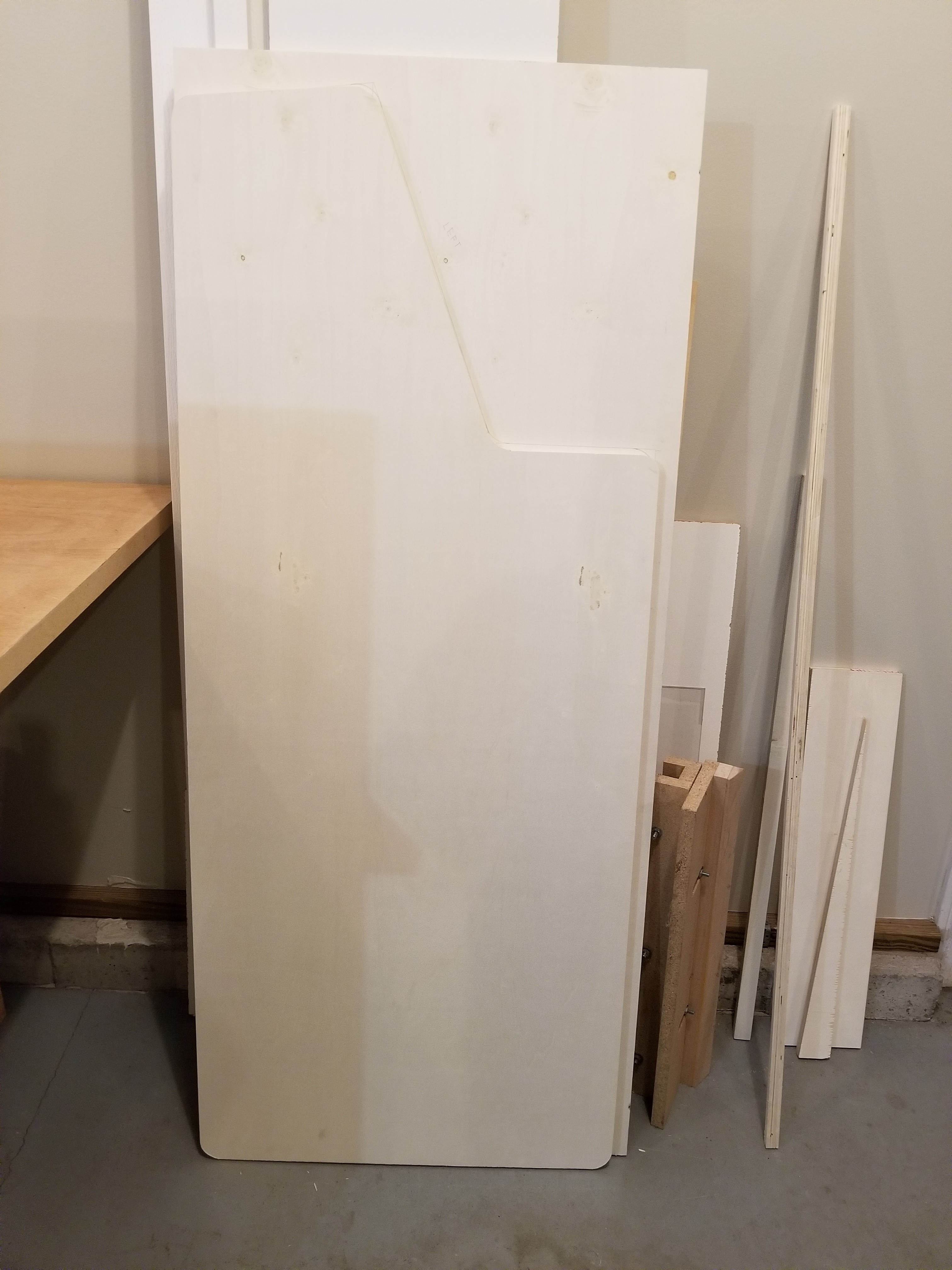
Here is the same side:
Next, we needed to rout grooves in the sides. We already decided that everything needed to be glued together. The grooves were perfect for that.
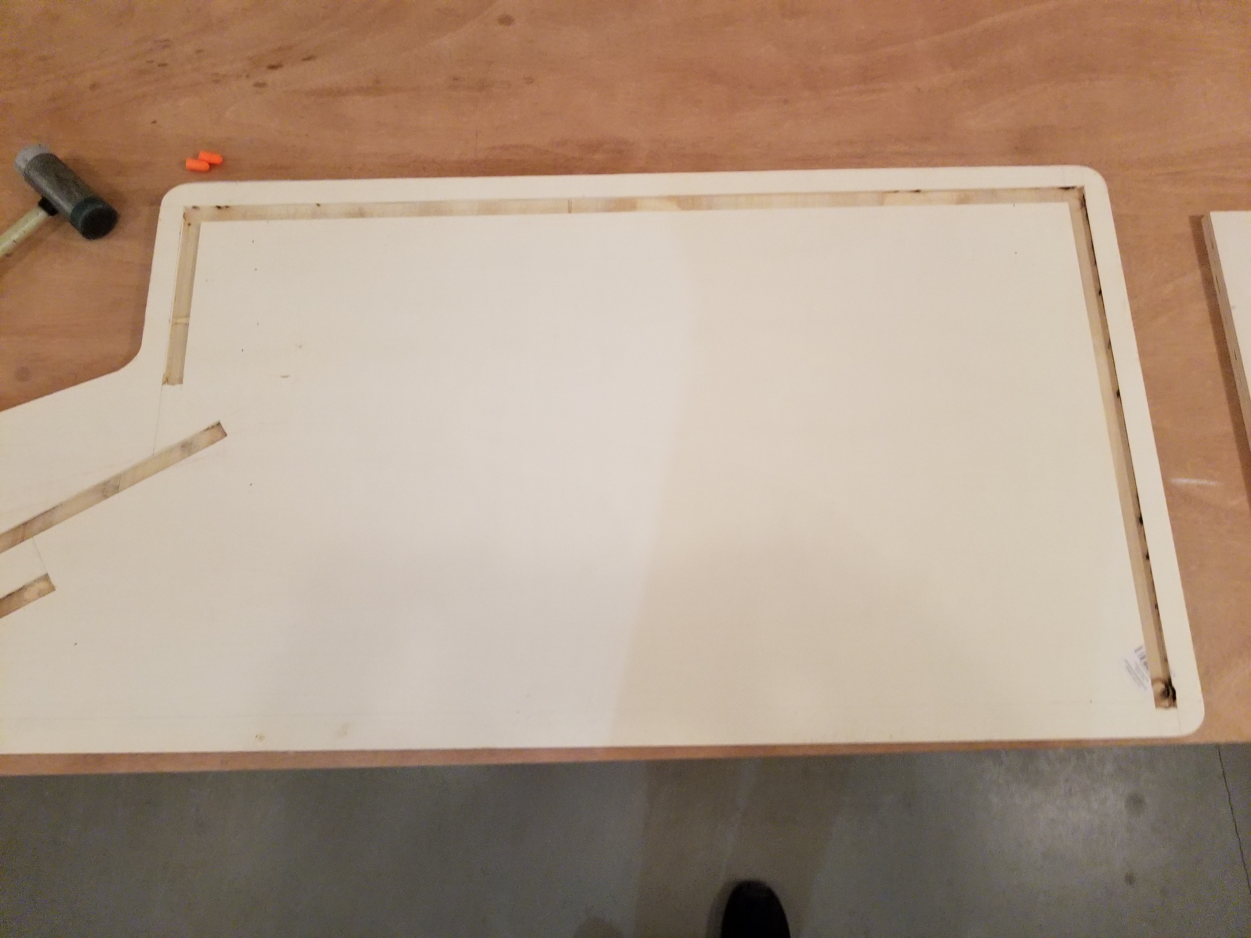
We weren't going to have a backdoor or anything like that.
From there, we proceeded to fit pieces and glue them in place.

Very pleased with the result:
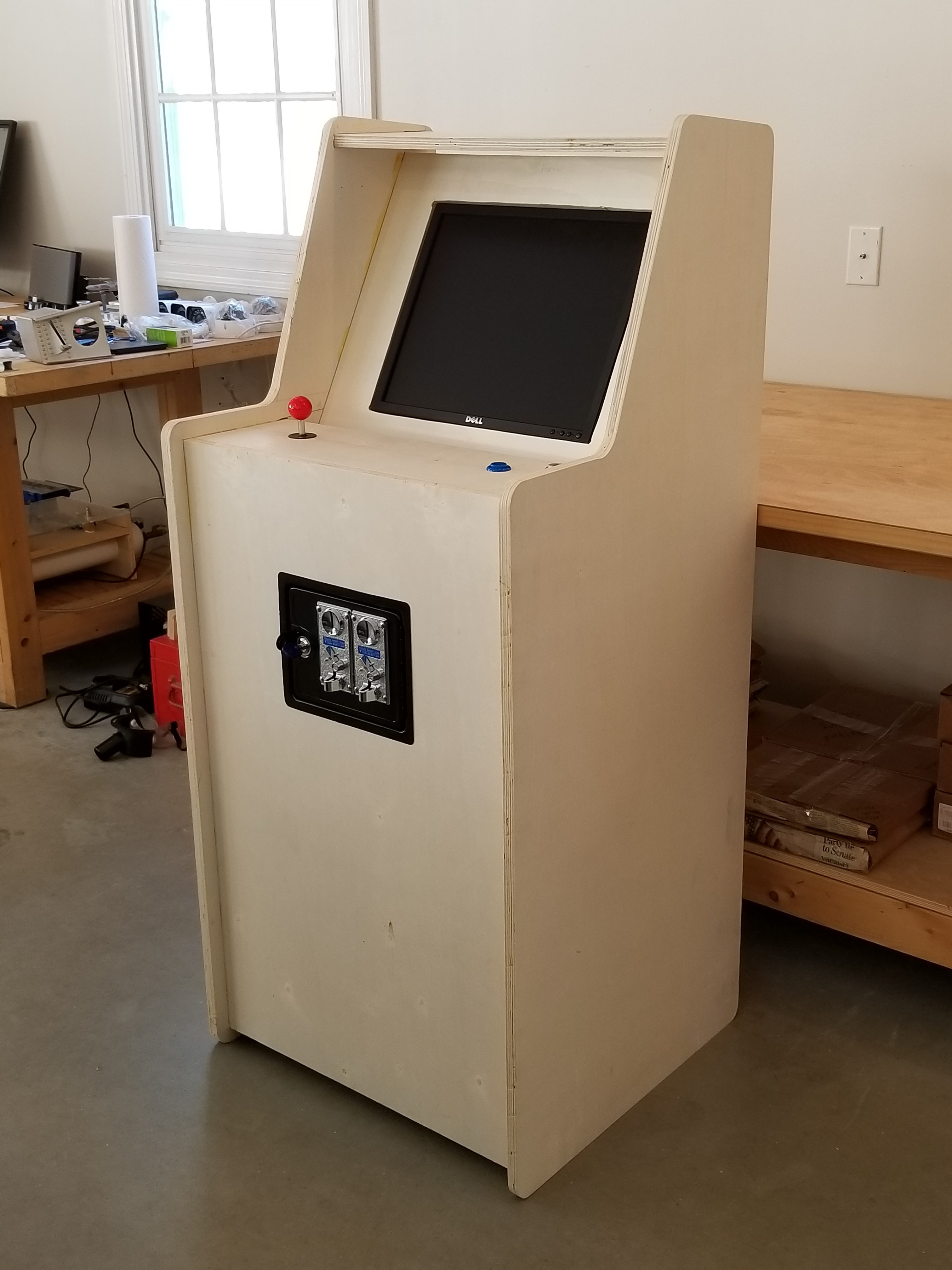
For the next several months, I used the cabinet to test my prototypes.
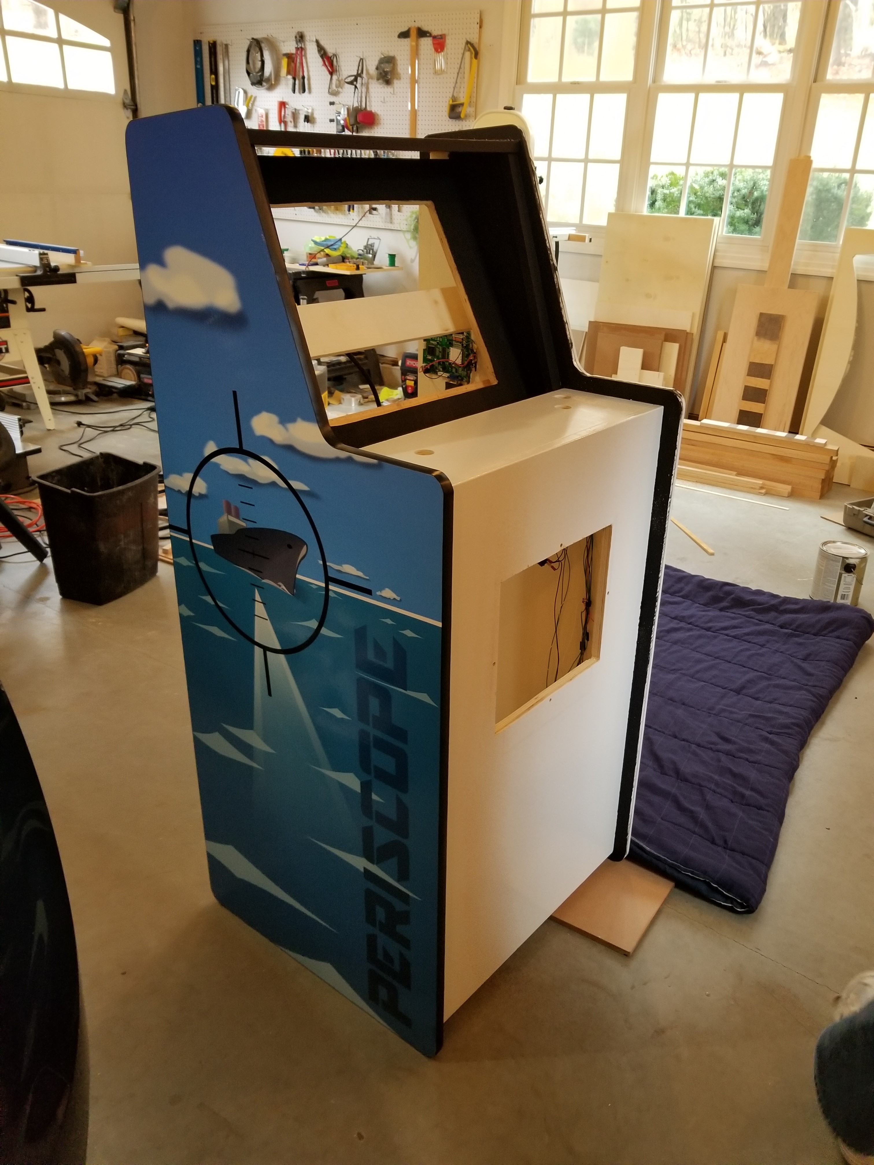
About a week before the Expo, art arrived. We started by priming the cabinet white, and then we began to place the art on the cabinet.
I think we can all agree: My Dad makes awesome art!
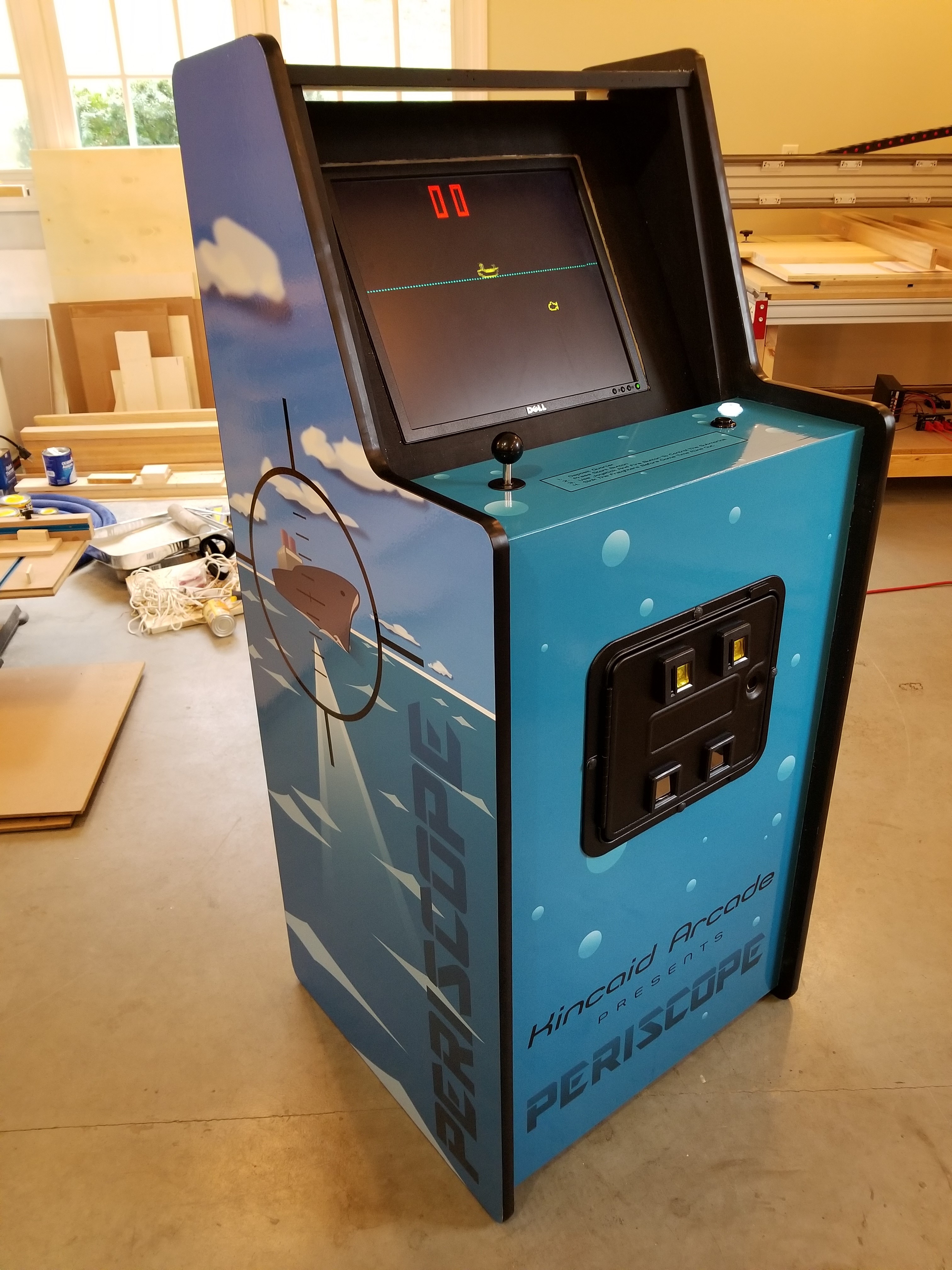
One last minor touch is needed: a bezel. After trying and trying to make a bezel, I finally got one that looked fine.
The rest is history:
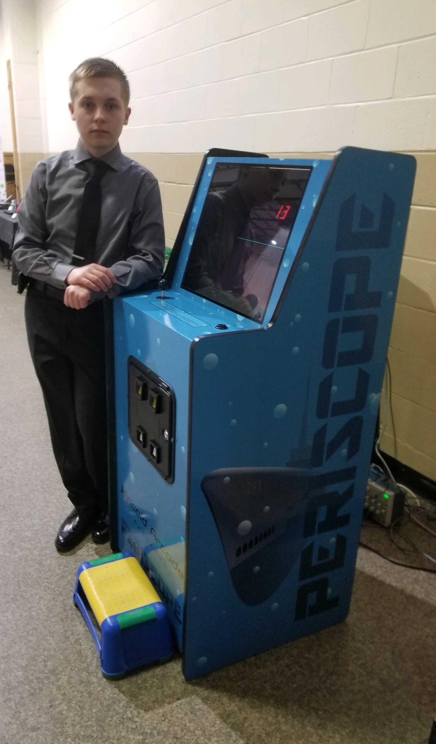
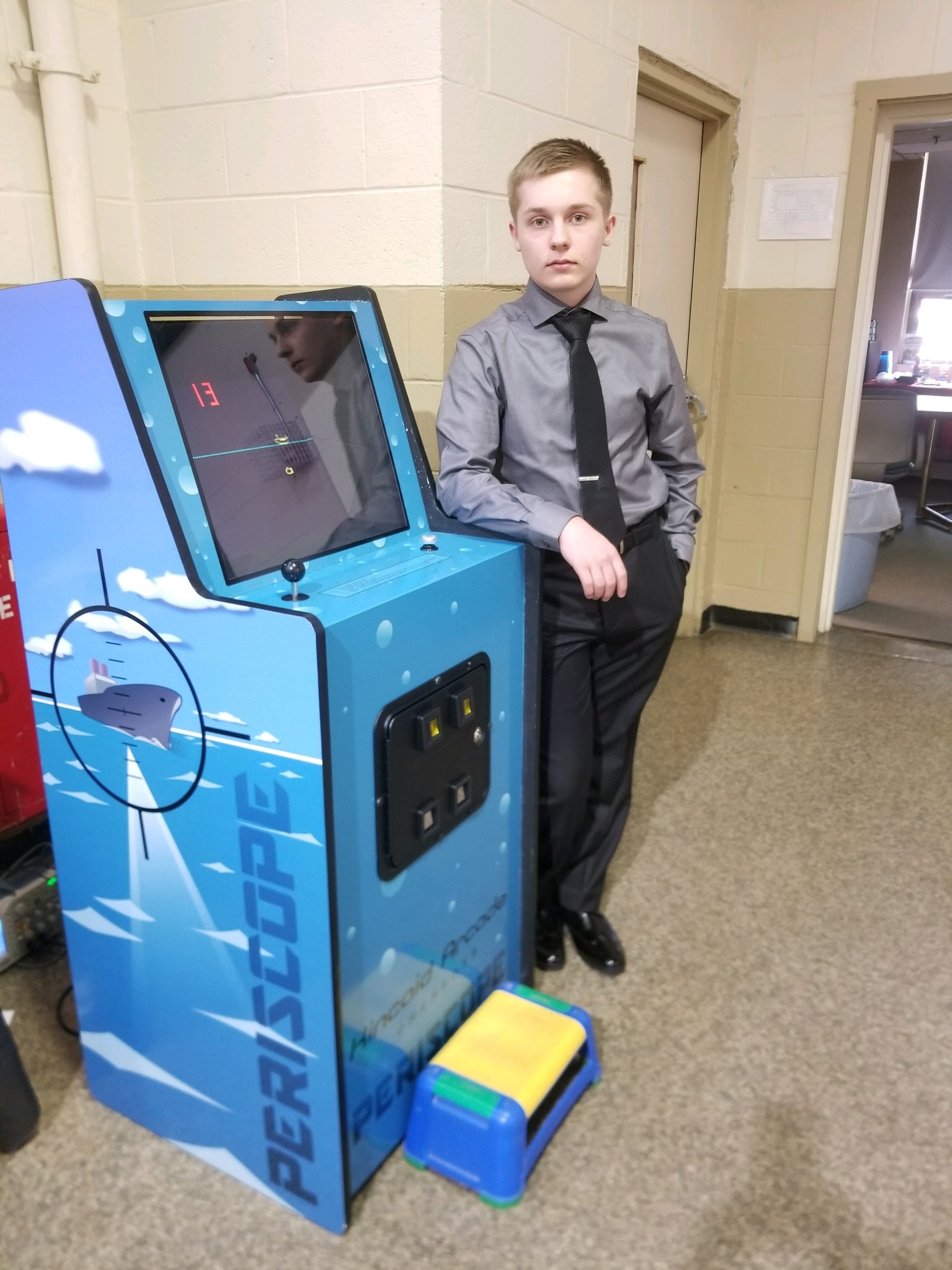
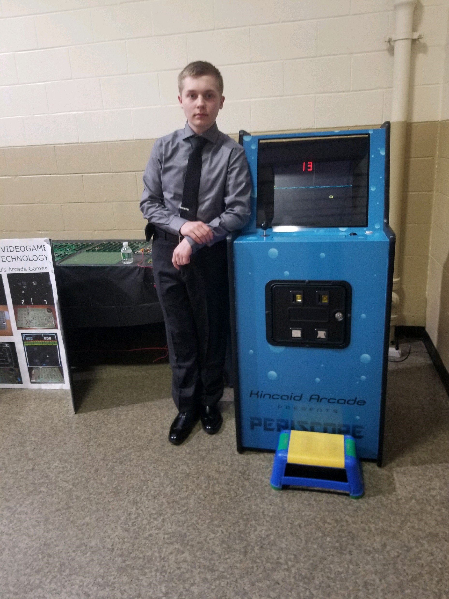
We always had to dress up for the exposition.
Gameplay Videos
I shot some gameplay videos with the help of my Mom.
When I scored 15 in the second video, I just beat my previous high score of 14. 15 is the world record now. I should really consider submitting a score to Twin Galaxies...
Reflection
In short, this was a great project.
This is the first school project I have completed to my satisfaction before the deadline. Usually, the projects need another 100 or so hours of time that I don't have. ~300 hours is about the most I can do in a schoolyear.
When working in my workroom. I listened to a lot of songs on endless loops.
- "Place In This World" - Michael W. Smith
- "Cross My Heart" - Michael W. Smith
- "Emily" - Michael W. Smith
- "Dare You To Move" - Switchfoot
Would I design another game? As much as I'd love to, there's no real reason to. A project like that would have to be commissioned by somebody else.
I've done some looking into how Vector games work, and yes, you could design one with TTL, however, drawing lines that aren't at right angles or 45 degree angles will be highly impractical.
I think I might just stick to doing another raster game.
I have been contemplating going out with a bang and doing an "Indy 800" difficulty game. (More than 14 PCBs)
Or just doing another game, to be housed in a PERISCOPE-style cabinet.
Either way, I already have a great game. So for now, I'll just put in another quarter and play.
This page was published during summer break of 2018.
This page was last updated 1/5/2022
Spelling, grammar, and readability corrections.